CXD9963GB
Jump to navigation
Jump to search
CXD9963GB


- Used on:
- PS3 Slim CECH-20xxA/B with motherboard DYN-001
- PS3 Slim CECH-21xxA/B with motherboard SUR-001
- PS3 Slim CECH-25xxA/B with motherboard JTP-001 or JSD-001
- PS3 Slim CECH-30xxA/B with motherboard KTE-001
- PS3 Super Slim CECH-40xxB with motherboard MSX-001
- PS3 Super Slim CECH-43xxA/B with motherboard REX-001
As these Motherboard Revisions/SKU Models do not have an USB hub chip, the frontports are directly connected to this South Bridge
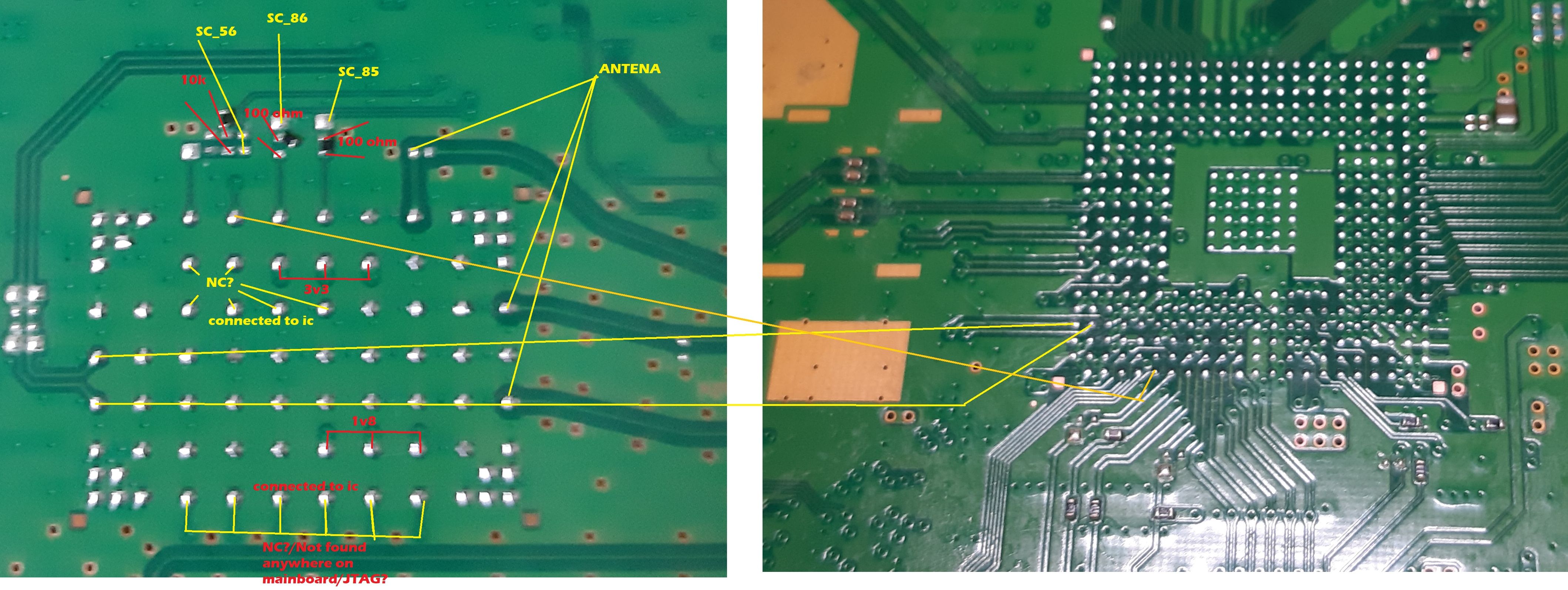
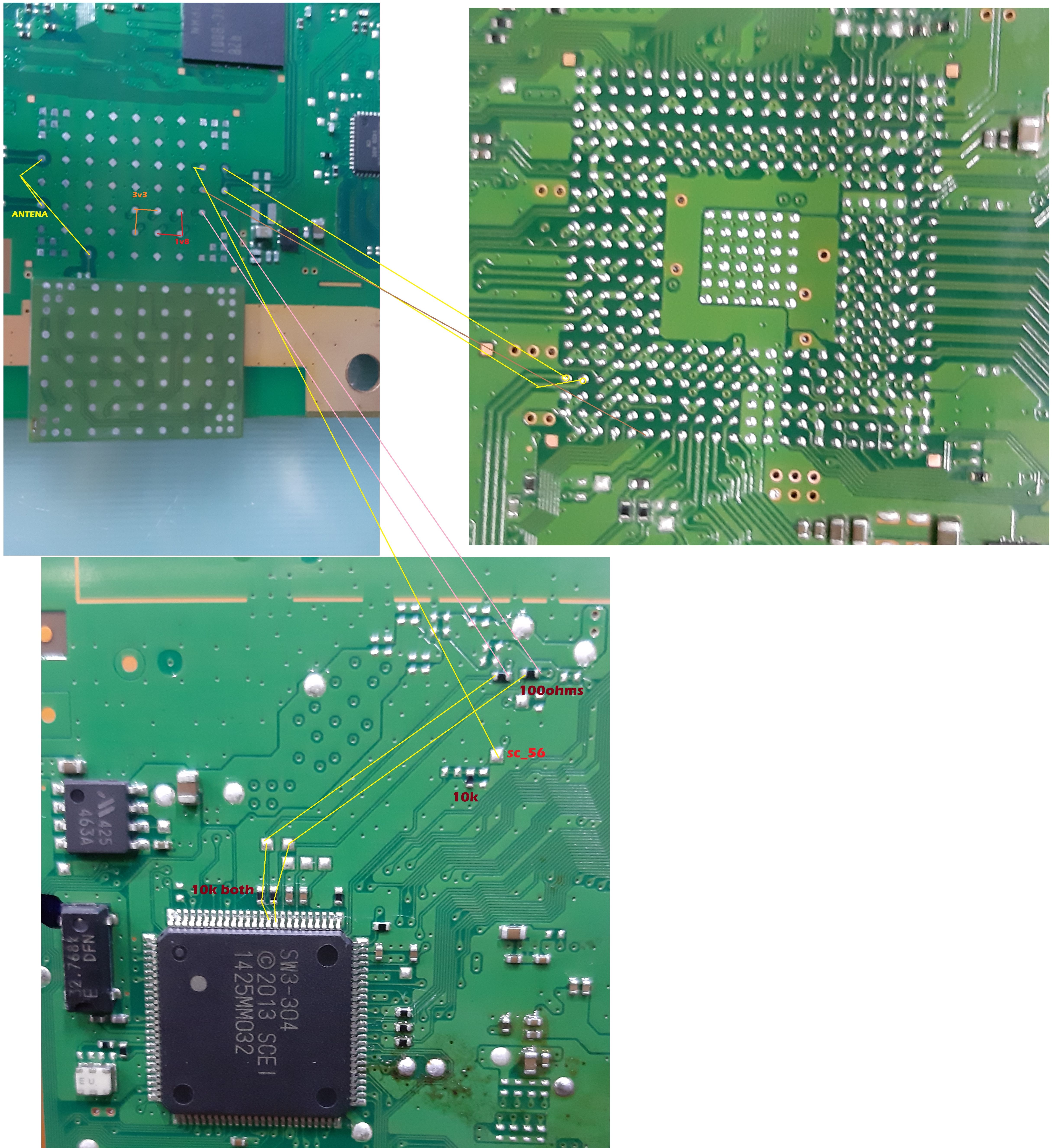
Pinout
| Pad# | Name | Port | Description |
|---|---|---|---|
| A4 | WIFI_DATA_1 | ? | Connected to wifi/BT module. See: wifi/BT 10x7 pinout or wifi/BT 9x7 pinout |
| B4 | WIFI_DATA_2 | ? | Connected to wifi/BT module. See: wifi/BT 10x7 pinout or wifi/BT 9x7 pinout |
| F1 | WIFI_CTRL | ? | Connected to wifi/BT module. See: wifi/BT 10x7 pinout or wifi/BT 9x7 pinout |
| This article is marked for rewrite/restructuring in proper wiki format. You can help PS3 Developer wiki by editing it. |
| |||||||||||||||||||||||||||||||||||||||||||||||||||||||||||||||||||||||||||||||||||||||||||||||||||||||||||||||||||||||||||||||||||||||||||||||||||||||||||||||||||||||||||||
