USB: Difference between revisions
mNo edit summary |
|||
| Line 57: | Line 57: | ||
Datasheet: http://www.ps3devwiki.com/files/documents/-Datasheets/USB/Genesys_Logic_GL852.pdf <br /> | Datasheet: http://www.ps3devwiki.com/files/documents/-Datasheets/USB/Genesys_Logic_GL852.pdf <br /> | ||
6-806-862-01 / IC3305 <br /> | 6-806-862-01 / IC3305 <br /> | ||
*Used in: | *Used in PS3 models: | ||
**[[CECHAxx]], [[CECHBxx]] (with [[COK-001]] motherboard) | **[[CECHAxx]], [[CECHBxx]] (with [[COK-001]] motherboard) | ||
| Line 123: | Line 123: | ||
=== GL852 (USB-Hub 64pin) === | === GL852 (USB-Hub 64pin) === | ||
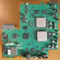
*Used in PS3 models: | |||
*Used in: | |||
**[[CECHCxx]], [[CECHExx]] (with [[COK-002]] motherboard) | **[[CECHCxx]], [[CECHExx]] (with [[COK-002]] motherboard) | ||
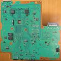
=== GL852 (USB-Hub 48pin) === | === GL852 (USB-Hub 48pin) === | ||
*Used in PS3 models: | |||
*Used in: | |||
**[[CECHGxx]] (with [[SEM-001]] motherboard) | **[[CECHGxx]] (with [[SEM-001]] motherboard) | ||
**[[CECHHxx]] (with [[DIA-001]] motherboard) | **[[CECHHxx]] (with [[DIA-001]] motherboard) | ||
Revision as of 14:15, 25 August 2015

USB 2.0
Depending on the SKU Models the PS3 is equiped with 6x (Tool/DECR), 4 or 2 USB (Universal Serial Bus) 2.0 ports with maximum bandwidth of 480 Mbit/s (~57 MB/s), connected internally to a USB-Hub chip.
Note: On PS3 Slim CECH-20xx/DYN-001 and later, the USB port datalines are directly connected to South Bridge without a USB-Hub chip (port is initialised via DC switch IC connected to South Bridge and TH3301 thermistor protect 5V input).
USB lines top view (common traces for all slim models)
USB lines bottom view (common traces for all slim models)
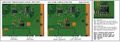
JSD-001/JTP-001 USB connector TH3301 thermistor and DC switch IC to South Bridge
.jpg)
.jpg)
Generic USB Pinout

| Pin | Color | Signal | Description |
|---|---|---|---|
| Shell | N / A | Shield | Metal housing |
| 1 | Red | VBUS | Power / +5 volt DC (max.500mA) |
| 2 | White | D- | USB 2.0 differential pair |
| 3 | Green | D+ | |
| 4 | Black | GND | Ground |
| Pin | Color | Signal | Description |
|---|---|---|---|
| Shell | N / A | Shield | Metal housing |
| 1 | Red | VBUS | Power |
| 2 | White | D- | USB 2.0 differential pair |
| 3 | Green | D+ | |
| 4 | N / A | ID | Permits detection of which end of a cable is plugged in: • "A" connector (host): connected to the signal ground • "B" connector (device): not connected |
| 5 | Black | GND | Ground |
Note: used on many Peripherals for charging/sync
Internal USB-Hub IC's


GL852-MSG02-MT (USB-Hub 64pin)
Datasheet: http://www.ps3devwiki.com/files/documents/-Datasheets/USB/Genesys_Logic_GL852.pdf
6-806-862-01 / IC3305
| Pin Name | 64 Pin# | 48Pin# | I/O Type | Description |
|---|---|---|---|---|
| DM0,DP0 | 3,4 | 3,4 | B | USB signals for USPORT |
| DM1,DP1 | 8,9 | 5,6 | B | USB signals for DSPORT1 |
| DM2,DP2 | 14,15 | 9,10 | B | USB signals for DSPORT2 |
| DM3,DP3 | 25,26 | 17,18 | B | USB signals for DSPORT3 |
| DM4,DP4 | 31,32 | 21,22 | B | USB signals for DSPORT4 |
| RREF | 17 | 11 | B | A 680Ω resister must be connected between RREF and analog ground (AGND). |
| OVCUR1#~4 | 56,54,42,40 | 42,40,30,28 | I (pu) |
Active low. Over current indicator for DSPORT1~4 OVCUR1# is the only over current flag for GANG mode. |
| PWREN1#~4 | 57,55,43,41 | 43,41,31,29 | O | Active low. Power enable output for DSPORT1~4 PWREN1# is the only power-enable output for GANG mode. |
| GREEN1~4 | 60,48,44,34 | 45,35,32,23 | 1,3,4: O 2: B (pd) |
Green LED indicator for DSPORT1~4 *GREEN[1~2] are also used to access the external EEPROM. For detailed information, please refer to Chapter 5. |
| AMBER1~4 | 61,49,45,35 | 46,36,33,24 | O (pd) |
Amber LED indicator for DSPORT1~4 *Amber [1~2] are also used to access the external EEPROM |
| PSELF | 50 | 37 | I | 0: GL852 is bus-powered. 1: GL852 is self-powered. |
| PGANG/ SUSPND |
53 | 39 | B | This pin is default put in input mode after power-on reset. Individual/gang mode is strapped during this period. After the strapping period, this pin will be set to output mode, and then output high for normal mode. When GL852 is suspended, this pin will output low. *For detailed explanation, please see Chapter 5 Gang input:1, output: 0@normal, 1@suspend |
| X1 | 20 | 14 | I | 12MHz crystal clock input. |
| X2 | 21 | 15 | O | 12MHz crystal clock output. |
| RESET# | 38 | 26 | I | Active low. External reset input, default pull high 10KΩ. When RESET# = low, whole chip is reset to the initial state. |
| TEST | 39 | 27 | I (pd) |
0: Normal operation. 1: Chip will be put in test mode. |
| AVDD | 11,18,22,28,64 | 1,7,12,16,19 | P | 3.3V analog power input for analog circuits. |
| AGND | 1,12,19,23,29 | 2,8,13,20 | P | Analog ground input for analog circuits. |
| DVDD | 37,47,52,59 | 25,34,38,44,48 | P | 3.3V digital power input for digital circuits |
| DGND | 36,46,51,58,62 | 47 | P | Digital ground input for digital circuits. |
| NC | 2,5~7,10,13,16,24,27,30,33 | - | - | No connection |
 Type
 O     Output
 I     Input
 B     Bi-directional
 B/I   Bi-directional, default input
 B/O   Bi-directional, default output
 P     Power / Ground
 A     Analog
 SO    Automatic output low when suspend
 pu    Internal pull up
 pd    Internal pull down
 odpu  Open drain with internal pull up
GL852 (USB-Hub 64pin)
GL852 (USB-Hub 48pin)
- Used in PS3 models:
| |||||||||||||||||||||||||||||||||||||||||||||||||||||||||||||||||||||||||||||||||||||||||||||||||||||||||||||||||||||||||||||||||||||||||||||||||||||||||||||||||||||||||||||
