88SA8040-TBC1: Difference between revisions
Jump to navigation
Jump to search
(Created page with "== Marvell 88SA8040-TBC1 == alt. part no: 88SA8040C0-TBC1C000-P107 (SATA 1.5 Gb/s to PATA 133) <br /> 6-710-129-01 / IC3401 <br /> SATA to PATA IDE bridge chip. This is u...") |
mNo edit summary |
||
| Line 1: | Line 1: | ||
== Marvell 88SA8040-TBC1 == | == Marvell 88SA8040-TBC1 == | ||
<div style="float:right">[[File:Marvell 88SA8040-TBC1.jpg|thumb|left|Marvell 88SA8040-TBC1]]<br />[[File:Marvell 88SA8052-pinout.png|thumb|left|Marvell 88SA8040/88SA8052 -TBC1 - pinout]]<br />[[File:Marvell 88SA8040-TBC1-pinout.jpg|thumb|left|Marvell 88SA8040/88SA8052 -TBC1 - application schematic]]</div> | |||
alt. part no: [[88SA8040C0-TBC1C000-P107]] (SATA 1.5 Gb/s to PATA 133) <br /> | alt. part no: [[88SA8040C0-TBC1C000-P107]] (SATA 1.5 Gb/s to PATA 133) <br /> | ||
6-710-129-01 / IC3401 <br /> | 6-710-129-01 / IC3401 <br /> | ||
| Line 18: | Line 20: | ||
input voltage 2.5V. Minimum input operating voltage is 2.5V.</pre> | input voltage 2.5V. Minimum input operating voltage is 2.5V.</pre> | ||
No datasheet found/available : http://www.marvell.com/storage/system-solutions/sata-to-pata-bridge.jsp <br /> | No datasheet found/available : http://www.marvell.com/storage/system-solutions/sata-to-pata-bridge.jsp <br /> | ||
Revision as of 13:52, 19 November 2012
Marvell 88SA8040-TBC1
alt. part no: 88SA8040C0-TBC1C000-P107 (SATA 1.5 Gb/s to PATA 133)
6-710-129-01 / IC3401
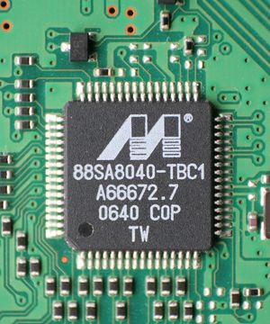
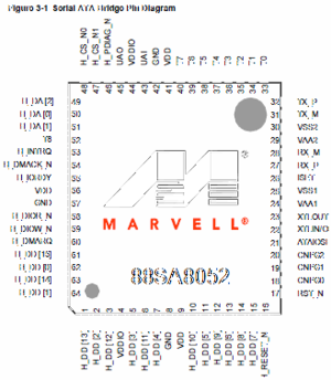
SATA to PATA IDE bridge chip. This is used on motherboards with a PATA blu-ray drive: early PS3 (up to including CECHKxx/DIA-002).
 The 88SA8040 is an IC which consists of 9 bus transceivers (three state output) in
 a 24 pin package. Signals are transmitter from A to B when the direction control
 input (DiR) is at a high level, and from B to A when DiR is at a low level. When the
 enable input (G) is high, A and B are isolated. And this product has two terminals
 (V CCA, VCCB), VCCA is connected with control input and A bus side, VCCB is connected
 with B bus side. VCCA and V CCB are isolated. Consequently, it is best to change the
 level in case of two supply voltage coexist on one board and application of power management.

 Dropout Voltage is defined as the input to output differential at which the output
 voltage drops 2% below its nominal value measured at 1V differential. For outputs below
 2.5V, dropout voltage is the input-to-output voltage differential with the minimum
 input voltage 2.5V. Minimum input operating voltage is 2.5V.
No datasheet found/available : http://www.marvell.com/storage/system-solutions/sata-to-pata-bridge.jsp


