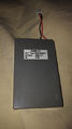
DualShock 3
Overview

CECH-ZC2J, CECH-ZC2JA, CECH-ZC2JB (CECH-ZC2U, CECH-ZC2E, CECH-ZC2J, CECH-ZC2H, CECH-ZC2M)
CECHZC2 (SCPH-98050, CBEH-1018: prototype)
FCC ID: AK8CECHZC2
ID: 409B-CECHZC2
MIC listings:
- 007WWCUL0622 February 28, 2011 (CECHZC2JA)
- 007WWCUL0622 April 12, 2012 (CECHZC2JA)
- 007WWCUL0622 September 20, 2012 (CECHZC2JA)
- 007-AB0090 April 26, 2013 (CECHZC2JA)
- 007WWCUL0686 June 16, 2011 (CECHZC2JB)
- 007WWCUL0241 October 3, 2007 (CECHZC2J)
- 007WWCUL0281 April 22, 2008 (CECHZC2J)
- 007WWCUL0324 October 21, 2008 (CECHZC2J)
- 007WWCUL0477 February 24, 2010 (CECHZC2J)
Anatel:
- 0516156223 30/03/2015 (CECHZC2M)
- 1745106223 13/06/2013 (CECHZC2M, CECHZC2U)
Patent:
| Model Number | Name description | Release date | Note |
|---|---|---|---|
| CECHZC2J | 2007, November 11 | Japan | |
| CECHZC2J SS | 2008, March 6 | Japan | |
| CECH-ZC2J MB | 2009, October 29 | Japan | |
| CECH-ZC2J DR | 2009, October 29 | Japan | |
| CECH-ZC2J LW | 2010, July 29 | Japan | |
| CECH-ZC2J CP | 2010, November 18 | Japan | |
| CECH-ZC2J YB | 2011, April 21 | Japan | |
| CECH-ZC2J JG | 2011, February 24 | Japan | |
| CEJH-15017 | TALES OF XILLIA®2 X cross Edition | 2012, November 1 | Japan |
| CEJH-15020 | God of War: Ascension bundle | 2013, March 14 | Japan |
| CECH-ZC2J MY | 2013, June 20 | Japan | |
| CECH-ZC2J VT | Vita TV edition (White) | 2013, November 14 | Japan |
| CECH-ZC2J CY | 2013, December 19 | Japan | |
- Regions (last letter of the "model number"):
- E Europe
- H Hong Kong
- HK Hong Kong
- J Japan
- K Korea
- R Russia
- T Taiwan
- U United States
- M Mexico (seen in Anatel.br)
- Revisions (small letter + number after the "model number")
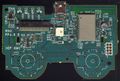
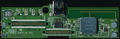
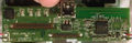
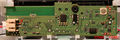
Controller Components
Printed Circuit Board (PCB) versions
PCB evolution
| MSU Versions |
Photos | Main Controller |
EEPROM | Power Control |
Sticks Control |
Motors Control |
Accelerometer | Gyroscope | BT Module |
Notes | |||||
|---|---|---|---|---|---|---|---|---|---|---|---|---|---|---|---|
| PP1.2 |  |
 |
Toshiba ? |
Renesas 504E |
Texas Instruments BKO |
? (3 pins pots) |
2x Unknown -KF (3 pins) |
Hokuriku HDK HAAM-325B (offboard) |
Murata ENC-03R (offboard) |
? | TYPE: Prototype MCU: Sensors connected to pins 77, 78, 79, 80, this doesnt matches with other models EEPROM: Renesas 504E, same one used in a lot of other next models POWER: Texas Instruments BKO controlls battery/USB charge STICKS: ALPS with 3 pins pots MOTORS: The -KF transistor is similar to the one used later in DualShock 3 ACCEL: HDK 325 (added manually) GYRO: Murata ENC-03R (added manually) BT: ? | ||||
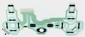
| PP4.0 5 | .jpg) |
.jpg) |
Toshiba T6UM2EFG 0103 |
Texas Instruments BKO ...and... 2x Ricoh P0NT ...and... 2x KEC ALG31 |
Texas Instruments YA018 (3 pins pots) |
No | Hokuriku HDK HAAM-325BA |
ALPS 103A |
TYPE: First retail sixaxis STICKS: Texas Instruments YA018 added to control sticks MOTORS: removed the -KF transistor and motors | ||||||
| PP4.0 9 | .jpg) |
.jpg) |
Toshiba T6UM3EFG 001 |
Hokuriku HDK HAAM-325BA ...or... Analog Devices 330K |
Murata ENC-03R ? (offboard) |
MCU: Toshiba controller was updated, maybe related with the new accelerometer TESTPOINTS: same location than PP4.0 5, but some removed | |||||||||
| PP4.0 11 | .jpg) |
.jpg) |
Hokuriku HDK HAAM-325BA ...or... Kionix KXPC4 |
TESTPOINTS: same location than PP4.0 9 | |||||||||||
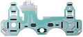
| V2 2.12 | .jpg) |
.jpg) |
Toshiba T6UN6EFG 001 |
Texas Instruments BKO ...and... NEC 871Y03 |
2x Toshiba 5W54 (4 pins pots) |
Epson-Toyocom X3500Z ? (offboard) |
ALPS 203A |
MCU: Toshiba controller was updated, maybe related with updated power or sticks POWER: NEC 871Y03 added STICKS: since this point the ALPS pots has 4 pins TESTPOINTS: new locations | |||||||
| V2 2.14 | .jpg) |
.jpg) |
2x Toshiba 763 (4 pins pots) |
Epson-Toyocom X3500Z ? (onboard) |
TESTPOINTS: same location as V2 2.12 | ||||||||||
| V2.5 1.05 | .jpg) |
.jpg) |
2x Toshiba 5W54 (4 pins pots) |
Kionix KXPC4 |
Epson-Toyocom X3500Z ? (offboard) |
ALPS 303A |
TESTPOINTS: same location as V2 2.12, but some removed and some renamed | ||||||||
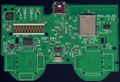
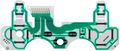
| VX 1.03 | .jpg) |
.jpg) |
Toshiba T6UN6EFG 002 |
NEC 871Y03 |
2x Unknown -KF ? (3 pins) |
Kionix KXSC4 |
Epson-Toyocom X3500Z ? (onboard) |
TYPE: First retail DualShock 3 MCU: Toshiba controller was updated, maybe related with new motor controllers TESTPOINTS: new locations | |||||||
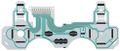
| V3.5X 1.12 | .jpg) |
.jpg) |
Texas Instruments B029 |
2x Unknown KEX (5 pins) |
Kionix KXSC4 ...or... STMicroelectronics 32S3 ? |
ALPS 413A |
TESTPOINTS: new locations | ||||||||
| V3.5X 1.14 | .jpg) |
.jpg) |
ALPS 113A |
TESTPOINTS: same location as V3.5X 1.12 | |||||||||||
| VX3 0.07 | .jpg) |
.jpg) |
Toshiba T6UN6EFG 003 |
Seiko Instruments S25C |
Texas Instruments SN84001 (4 pins pots) |
Kionix KXSC4 ...or... STMicroelectronics unknown |
ALPS 413A |
MCU: Since this point pins 37, 38, 39, 40 are connected to a resistors network and to the sticks controller TESTPOINTS: new locations | |||||||
| VX3 0.08 | .jpg) |
.jpg) |
Texas Instruments B029A |
Epson-Toyocom X3500Z ? (offboard) |
TESTPOINTS: same location as VX3 0.07 | ||||||||||
| VX3 0.11 | .jpg) |
.jpg) |
Kionix KXSC4 ...or... STMicroelectronics 32S3 |
Epson-Toyocom X3500Z ? (onboard) |
TESTPOINTS: same location as VX3 0.07 | ||||||||||
| VX4 0.09 | .jpg) |
.jpg) |
Texas Instruments R2A20060 |
STMicroelectronics Y35A ? (offboard) |
TESTPOINTS: new locations | ||||||||||
| VX4 0.10 | .jpg) |
.jpg) |
Seiko Instruments S25C ...or... STMicroelectronics 504RP |
Texas Instruments SN89062 |
STMicroelectronics Y35A (onboard) |
TESTPOINTS: same location as VX4 0.09 | |||||||||
| VX5 0.05 | .jpg) |
.jpg) |
Texas Instruments A6044A0 (power and 4 pins pots) |
ALPS 603A |
TESTPOINTS: new locations | ||||||||||
| VX5 0.06 | .jpg) |
.jpg) |
STMicroelectronics Y35A ? (offboard) |
TESTPOINTS: same location as VX5 0.05 | |||||||||||
| VX6 0.06 | .jpg) |
.jpg) |
Texas Instruments SN89062 |
? (3 pins pots) |
MCU: Since this point pins 37, 38, 39, 40 has been repurposed TESTPOINTS: same location as VX5 0.05, but a lot of renamed | ||||||||||
| VX7 0.04 | .jpg) |
.jpg) |
STMicroelectronics 504RP |
2x Unknown KE4 (5 pins) |
STMicroelectronics Y35A (onboard) |
TESTPOINTS: new locations STICKS: Analogue sticks are no longer soldered, instead are now friction fit to the second ribbon cables with a piece of rubber. PCB: Now uses a rubber piece instead of foam to hold the ribbon cables against the PCB. | |||||||||
| VX8 0.14 | .jpg) |
.jpg) |
? | STMicroelectronics 432RK |
? | CSR BlueCore Unknown |
TESTPOINTS: new locations Usually found in CECHZC2_A2 revision controllers | ||||||||
| MSU Versions |
Photos | Main Controller |
EEPROM | Power Control |
Sticks Control |
Motors Control |
Accelerometer | Gyroscope | BT Module |
Notes | |||||
Prototypes
PP1
- Models
- MSU PP1.2 MAIN ALPS
Notable differences include
- Plastic finish being glossy
- Player LEDs arranged in a square around the USB-mini port and includes a clear plastic shield over the opening for the LEDs
- PS Home button is clear and retains a red LED underneath it
- L2 and R2 buttons are present as opposed to Triggers
- Motors are present
- Battery inside contains a sticker with the date 2006/3/2 and the model of the batter appears to be longer
- Lacks the pinhole and switch on the back
- Label on the front reads Gセンサー搭載 Stick動作せず once roughly translated it reads Powered by the G Sensor, without moving the stick
- Label on the back reads 0604KATA2
- Toshiba MCU is on top side of the board (in all the other models is at bottom)
- The main board was designed without gyroscope and without accelerometer sensors, it has a "children board" sticked on top manufactured by HDK (the first 2 letters of the "HDK" brand are partially visible etched on copper on the children board), this children board includes the accelerometer HDK HAAM 325B [1]. It outputs 3 signals on the 3 white wires "hand made" soldered to the TOSHIBA controller to retrieve the axis data. The other "hand made" soldered component uses 3 wires (black = ground, red = volts, and yellow soldered to TP26) seems to be a Murata ENC-03R Gyroscope Sensor [2]. It seems both components was integrated later in the circuit board of the controllers labeled "sixaxis"
Internally the Gyroscopic sensor for Sixaxis controllers is wired onto the board - presumably as a test for a sensor revision on a spare sample board. The sensor itself appears to be far from complete and very early. Windows (10) detects the controller when connected via USB; analog sticks do not get detected but all other buttons do. The controller does not work on DECHA00A/J units, but might work on DECR units or earlier.
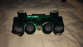
Front comparison next to a CECHZC2U
Back comparison next to a CECHZC2U
Top comparison to a CECHZC2U
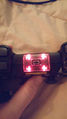
Front LED
Top LEDs
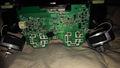
Back of the Board
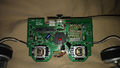
Front of the Board
Gyro Sensor. Click to see it in detail
Battery found inside


Sixaxis
PP4
- Models
- MSUPP4.0 5 http://www.kako.com/neta/2006-018/2006-018.html
- MSUPP4.0 9
- MSUPP4.0 11
MSU PP4.0 5
(Top)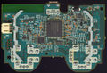
MSU PP4.0 5
(Bottom)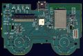
MSU PP4.0 9
(Top)
MSU PP4.0 9
(Bottom)
MSU PP4.0 11
(Top)
MSU PP4.0 11
(Bottom)
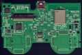
V2
- Models
- MSU_V2 2.12
- MSU_V2 2.14
Notable differences
- Sticks potenciometers with 4 legs, previous versions had 3 legs
MSU_V2 2.12
(Top)
MSU_V2 2.12
(Bottom)
MSU_V2 2.14
(Top)
MSU_V2 2.14
(Bottom)
V2.5
- Models
- MSU_V2.5 1.05
MSU_V2.5 1.05
(Top)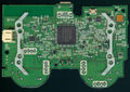
MSU_V2.5 1.05
(Bottom)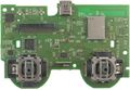
MSU V2.5 1.05
(Top) BIG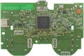
MSU V2.5 1.05
(Bottom) BIG
_BIG.jpg)
_BIG.jpg)
DualShock 3
VX
- Models
- MSU_VX 1.03
Notable differences
- Added vibration motors
- Updated wireless module
MSU_VX 1.03
(Top)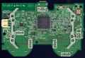
MSU_VX 1.03
(Bottom)
V3.5X
- Models
- MSU_V3.5X 1.12
- MSU_V3.5X 1.14
Notable differences
- Pressure connector for the buttons membrane
MSU_V3.5X 1.12
(Top)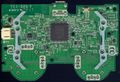
MSU_V3.5X 1.12
(Bottom)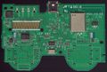
MSU_V3.5X 1.14
(Top)
MSU_V3.5X 1.14
(Bottom)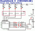
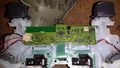
Dualshock 3 digital buttons and LED's interfacing
MSU_V3.5X board

VX3
- Models
- MSU_VX3_0.07
- MSU_VX3_0.08
- MSU_VX3_0.11
MSU_VX3_0.07
(Top)
MSU_VX3_0.07
(Bottom)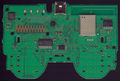
MSU_VX3_0.08
(Top)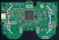
MSU_VX3_0.08
(Bottom)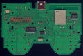
MSU_VX3_0.11
(Top)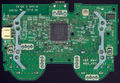
MSU_VX3_0.11
(Bottom)
VX4
- Models
- MSU_VX4_0.09
- MSU_VX4_0.10
MSU_VX4_0.09
(Top)
MSU_VX4_0.09
(Bottom)
MSU_VX4_0.10
(Top)
MSU_VX4_0.10
(Bottom)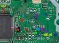
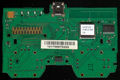
Dualshock 3 MSU VX4 buttons alternative points

VX5
- Models
- MSU_VX5_0.05
- MSU_VX5_0.06
Notable differences
- Updated wireless module
MSU_VX5_0.05
(Top)
MSU_VX5_0.05
(Bottom)
MSU_VX5_0.06
(Top)
MSU_VX5_0.06
(Bottom)
VX6
- Models
- VX6_0.06
Notable differences
- Sticks potenciometers with 3 legs, previous versions had 4 legs
MSU_VX6_0.06
(Top)
MSU_VX6_0.06
(Bottom)
Dualshock 3 VX6 board, accelerometer traces detail

VX7
- Models
- MSU_VX7_0.04
PCB is multilayer
MSU_VX7_0.04
(Top)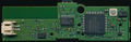
MSU_VX7_0.04
(Bottom)
VX8
There is not much info about this model, so is not clear if is the official VX8 or a third party clone of VX7The VX8 is official, the board traces, testpoint locations, and the sensor chips has a lot of coincidences with VX7... the weird thing that is shocking is the toshiba chip and the alps bluetooth module has been replaced. The PCB has more than 2 layers (previous versions up to VX6 had only 2 layers)
MSU VX8 0.14 (top)
MSU VX8 0.14 (bottom)
MSU_VX8_?.??
(Bottom)
.jpg)
Others
Asuka
The ASUKA boards made in china seems to be 3rd party (not sony official). At the time when was released sony was manufacturing the VX5 series... later sony continued with VX6, VX7, etc... ignoring the "ASUKA" labeling
- Models
- ASUKA REV: 1.06
- ASUKA REV: 1.07
ASUKA REV: 1.06
(Top)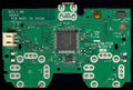
ASUKA REV: 1.06
(Bottom)
.jpg)
.jpg)
PCB TestPoints
| Controller Type | Prototype | Sixaxis | DualShock 3 | ASUKA | |||||||||||
|---|---|---|---|---|---|---|---|---|---|---|---|---|---|---|---|
| TestPoints Relocations | 0 | 1 | 2 | 3 | 4 | 5 | 6 | 7 | 8 | NO | |||||
| Board Model | PP1 | PP4- | PP4+ | V2 | V2.5 | VX | V3.5X | VX3 | VX4 | VX5 | VX6 | VX7 | VX8 | 1.06 | 1.07 |
| Total amount of testpoints | 26 | 26 | 26 | 4 | |||||||||||
| USB +5V | TP4 ? | TP1 | TP1 | TP1 | TP1 | TP1 | TP1 | TP1 | TP1 | TP1 | TP1 | UNL | T207 | ||
| USB Data - | TP2 | TP2 | TP2 | TP2 | TP2 | TP2 | TP2 | TP2 | TP2 | TP2 | TP2 | UNL | T206 | ||
| USB Data + | TP3 | TP3 | TP3 | TP3 | TP3 | TP3 | TP3 | TP3 | TP3 | TP3 | TP3 | UNL | T205 | ||
| USB Ground (or Common Ground) | 4x GND | TP21, TP22, TP23, TP24 | TP4, TP5, TP6, TP7 | 4x GND | 4x UNL | T509 | |||||||||
| Battery USB power good ? | TP6 ? | N/A | |||||||||||||
| Battery charge start ? | TP7 ? | N/A | |||||||||||||
| Battery charge setpoint pre ? | TP9 | N/A | |||||||||||||
| Battery charge setpoint post ? | TP64 ? | N/A | |||||||||||||
| Battery status 1 ? | TP8 ? | TP8 | TP15 | TP31 | UNL | ||||||||||
| Battery status 2 ? | TP10 ? | TP9 | TP9 | TP32 | UNL | ||||||||||
| 2.8V Switched. Power for vibration motors | 3.0V ? | N/A | TP42 | TP8 | TP25 | UNL | T501 | ||||||||
| Bluetooth Module, unknown | TP10 | TP11 | TP26 | T504 ? | |||||||||||
| 2.8V Standby. Power for MCU, EEPROM, BT, |
TP10 | TP10 | TP62 | TP62 | TP62 | TP51 | TP11 | TP11 | TP10 | TP29 | T507 | T507 | |||
| 2.8V Switched. Power for Accelerometer and Gyroscope | TP12 | TP12 | TP28 | UNL | T506 | T506 | |||||||||
| 2.8V Switched. Power for 4x Stick |
TP13 | TP13 | TP13 | TP27 | UNL | T505 | |||||||||
| 3.7V Battery + | TP5 ? | TP14 | TP14 | TP14 | TP30 | UNL | T508 | ||||||||
| COM 1. Common Line for Analog |
TP21 ? | TP17 | TP17 | TP25 | TP25 | TP25 | TP17 | TP17 | TP17 | TP17 | TP14 | UNL | T101 | ||
| COM 2. Common Line for Analog |
TP22 ? | TP18 | TP18 | TP26 | TP26 | TP26 | TP18 | TP18 | TP18 | TP18 | TP15 | UNL | T102 | ||
| COM 3. Common Line for Digital |
TP60 | TP60 | N/A | ||||||||||||
| TP19 ? | TP27 ? | TP19 ? | TP19 ? | TP19 ? | TP19 ? | TP16 ? | UNL | T103 | |||||||
| TP20 ? | TP28 ? | TP20 ? | TP20 ? | TP20 ? | TP20 ? | TP17 ? | UNL | T104 | |||||||
| TP21 ? | TP29 ? | TP21 ? | TP21 ? | TP21 ? | TP21 ? | TP18 ? | UNL | T105 | |||||||
| TP22 ? | TP30 ? | TP22 ? | TP22 ? | TP22 ? | TP22 ? | TP19 ? | UNL | T106 | |||||||
| Toshiba T6UN6EFG pin 69, unknown | TP23 | N/A ? | TP23 | TP23 | TP23 | TP20 | |||||||||
| Toshiba T6UN2EFG pin 68 | TP24 | TP24 | TP31 ? | TP31 ? | TP31 ? | TP23 ? | N/A | ||||||||
| Unknown (Toshiba T6UN6EFG pin 67 ?) | TP25 | TP25 | TP37 ? | TP37 ? | TP37 ? | TP29 ? | N/A | ||||||||
| Unknown | TP36 | TP36 | TP44 ? | TP44 ? | TP44 ? | TP36 ? | N/A | ||||||||
| TP26 | TP26 | TP32 | TP32 | TP32 | TP24 | N/A | |||||||||
| TP27 | TP27 | TP33 | TP33 | TP33 | TP25 | N/A | |||||||||
| TP28 | TP28 | TP34 | TP34 | TP34 | TP26 | N/A | |||||||||
| TP29 | TP29 | TP35 | TP35 | TP35 | TP27 | N/A | |||||||||
| TP30 | TP30 | TP36 | TP36 | TP36 | TP28 | N/A | |||||||||
| TP37 | TP37 | TP38 | TP38 | TP38 | TP30 | N/A | |||||||||
| TP31 | TP31 | TP39 | TP39 | TP39 | TP31 | N/A | |||||||||
| TP38 | TP38 | TP40 | TP40 | TP40 | TP32 | N/A | |||||||||
| TP39 | TP39 | TP41 | TP41 | TP41 | TP33 | N/A | |||||||||
| TP32 | TP32 | TP42 | TP42 | TP42 | TP34 | N/A | |||||||||
| TP33 | TP33 | TP43 | TP43 | TP43 | TP35 | N/A | |||||||||
| TP34 | TP34 | TP45 | TP45 | TP45 | TP37 | N/A | |||||||||
| TP41 | TP41 | TP46 | TP46 | TP46 | TP38 | N/A | |||||||||
| TP35 | TP35 | TP47 | TP47 | TP47 | TP39 | N/A | |||||||||
| TP42 | TP42 | TP48 | TP48 | TP48 | TP40 | N/A | |||||||||
| TP43 | TP43 | TP49 | TP49 | TP49 | TP41 | N/A | |||||||||
| TP44 | TP44 | TP50 | TP50 | TP50 | TP42 | N/A | |||||||||
| Bluetooth module (SPI unknown 1) | S-CL ? | CON | TP74 | TP47 | UNL | TP23 | UNL ? | ||||||||
| Bluetooth module (SPI unknown 2) | S-CS ? | CON | TP75 | TP48 | UNL | TP24 | UNL ? | ||||||||
| Bluetooth module (SPI unknown 3) | S-MI ? | CON | TP76 | TP49 | UNL | TP25 | UNL ? | ||||||||
| Bluetooth module (SPI unknown 4) | S-MO ? | CON | TP77 | TP50 | UNL | TP26 | UNL ? | ||||||||
| Accelerometer Y-Axis (raw signal) | TP32 | TP32 | TP8 | UNL | T302 | ||||||||||
| Accelerometer X-Axis (raw signal) | TP33 | TP33 | TP9 | UNL | T303 | ||||||||||
| Accelerometer Z-Axis (raw signal) | TP34 | TP34 | TP10 | UNL | T301 | ||||||||||
| Accelerometer Y-Axis (filtered signal) | TP54 ? | TP35 | TP35 | TP11 | UNL | T305 | |||||||||
| Accelerometer X-Axis (filtered signal) | TP55 ? | TP36 | TP36 | TP12 | UNL | T306 | |||||||||
| Accelerometer Z-Axis (filtered signal) | TP56 ? | TP37 | TP37 | TP13 | UNL | T304 | |||||||||
| Gyroscope (filtered signal) | TP40 | TP40 | TP33 | ||||||||||||
| Gyroscope (raw signal) | TP26 ? | TP41 | TP41 | TP34 | |||||||||||
| Enable Small motor | TP54 | N/A | N/A | ||||||||||||
| Enable Big motor | TP15 | N/A | N/A | ||||||||||||
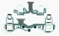
Ribbon Circuit Boards
For any arcade stick builders soldering to the vias on the PCB board (in the models where there are no testpoints availables) isn't exactly the easiest thing to do, using the copper contacts for the ribbon board is really the best option. In some board models (VX3, VX4, VX5, VX6, VX8) the copper contacts are covered by a black carbon material that needs to be removed if these spots are to be used to solder in them, this can be done with an X-acto knife or some fine sandpaper, just be careful and when you get to the shiny copper, STOP, you're done. Tin it up with some solder and there are your spots to use. Try and use a 30awg wire, or 28awg at the largest, and make sure to secure the wiring with some hot glue after you make the connection, but don't glue over the solder joint you just made, secure the wire to the board back from the solder joint, in case you ever have to get to it again for any reason.
The pull-up 7.5k Resistors ("printed" on the ribbon circuit boards) also need to be put back in the circuit as they're built into the ribbon board and when it's removed they're not, and the controller will act up on you if these are not in the circuit. There needs to be 2 of these pull-up resistors installed, one goes from V_STBY to COM1, the other goes from V_STBY to COM2. If you don't have any 7.5k resistors you can use anything from 6.8k to 10k really, but they do need to be installed since the ribbon board is removed when building an arcade stick, all of the PS3 controllers are setup this way and need those pull-up resistors if the ribbon board is removed
| PCB | Ribbon | Compatibility | Notes |
|---|---|---|---|
| ? | SA1Q135A | for sixaxis | |
| VX | SA1Q146A | The first dualshock 3 model | |
| ? | SA1Q159A | Yes | |
| ? | SA1Q160A | ||
| ? | SA1Q188A | ||
| VX4 | SA1Q189A | shipped with a CECH-2504 datecode 0C. Seems to be identical to SA1Q188A | |
| VX5 | SA1Q194A | not compatible with previous models, PS button changes | |
| ? | SA1Q195A | ||
| VX7 ? | SA1Q222A | Yes | superslims date ?. Is composed by 2 separated ribbons |
| ? | SA1Q224A | superslims date ?. Is composed by 2 separated ribbons |
SA1Q135A
Sixaxis Ribbon Circuit Board SA1Q135A

SA1Q146A
SA1Q159A
Dualshock 3 Ribbon Circuit Board SA1Q159A

SA1Q160A
Dualshock 3 Ribbon Circuit Board SA1Q160A

Counting from left to right... pins 8 and 14 are connected together in the PCB and carries 2.8v stanbdy (in the PCB the copper traces are wider than the others for this reason), This means there is a voltage permanently on this ribbon, also the ![]() button "wakes up" the controller from standby by sending this voltage back to toshiba chip
button "wakes up" the controller from standby by sending this voltage back to toshiba chip
SA1Q188A
Dualshock 3 Ribbon Circuit Board SA1Q188A

SA1Q189A
SA1Q194A
Dualshock 3 Ribbon Circuit Board SA1Q194A

SA1Q195A
SA1Q222A
Dualshock 3 Ribbon Circuit Board SA1Q222A

SA1Q224A
Battery
Li-Ion (Accupack)
LIP1359
Shipped with VX4 boards
MODEL LIP1359 Li-ion
BATTERY PACK 3.7V(3,7V)570mAh/2.1Wh
(typ. 610mAh)
Maximun Charge Current: 0.4 A
Maximun Charge Voltage: 4.2 V
LIP1472
Shipped with VX5 boards
MODEL LIP1472 Li-ion
BATTERY PACK 3.7V(3,7V)570mAh/2.1Wh
(typ. 610mAh)
Maximun Charge Current: 0.7 A
Maximun Charge Voltage: 4.25 V
LIP1859
MK11-2902
3.7V 610mAh
MK11-3020
3.7V 570mAh (typ. 610mAh)
Printed Circuit Board Components
MicroController Unit (MCU)
QFP package, 80pin
The pinout of the Toshiba T6UN6EFG-003 was traced in a VX4 board. Has not been verifyed if the pinout matches with T6UN6EFG-001 or T6UN6EFG-002 or other boards. It seems the pins can be remapped at bootloder as can be seen in the photos of the PP1 prototype (note the sensors in that photo are connected to pins 77, 78, 79, 80, this doesnt matches with newer dualshocks 3 models). Some people said in most older versions of the controller it was posible to update the controller firmware by USB with a tool that uploads a rom to the controller, this update procedure should be made by using the BT module because all USB connections are managed by it (so in some way it was the BT module the responsible to update the toshiba controller)
Toshiba T6UM2EFG

T6UM2EFG-0103
Toshiba T6UM3EFG

T6UM3EFG-001 Used in the sisaxis controllers shipped with the first european PS3 models
Toshiba T6UN6EFG


- Submodels:
- Toshiba T6UN6EFG-001
- Toshiba T6UN6EFG-002
- Toshiba T6UN6EFG-003
| Pin # | Name | Port | Description |
|---|---|---|---|
| 1 | GND | To ground | |
| 2 | V_STBY | 2.8V Standby. Power for Toshiba T6UN6EFG, EEPROM, | |
| 3 | GND | To ground | |
| 4 | V_BATT | 2x Capacitor network to ground, and resistor to battery and Texas Instruments SN89062 pin 16 in VX4 boards | |
| 5 | V_STBY | 2.8V Standby. Power for Toshiba T6UN6EFG, EEPROM, | |
| 6 | SENSOR_ACCL_X | To acccelerometer X axis through resistor | |
| 7 | SENSOR_ACCL_Y | To acccelerometer Y axis through resistor | |
| 8 | SENSOR_ACCL_Z | To acccelerometer Z axis through resistor | |
| 9 | SENSOR_GYRO | To gyroscope through resistor | |
| 10 | V_STBY | 2.8V Standby. Power for Toshiba T6UN6EFG, EEPROM, | |
| 11 | SLAVES_RESET | Texas Instruments SN84001 pin 2, and ALPS 413A pin 5 through resistor network in VX4 boards | |
| 12 | GND | To ground | |
| 13 | BT_POWER_CTRL ? | Texas Instruments SN89062, pin 4 in VX4 boards | |
| 14 | BT_UART_1 ? | To BT module (ALPS 413A pin 8 in VX4 boards) through resistor | |
| 15 | BT_UART_2 ? | To BT module (ALPS 413A pin 6 in VX4 boards) through 4x resistor network | |
| 16 | BT_UART_3 ? | To BT module (ALPS 413A pin 9 in VX4 boards) through 4x resistor network | |
| 17 | BT_UART_4 ? | To BT module (ALPS 413A pin 7 in VX4 boards) | |
| 18 | BT_UNK_1 | To BT module (ALPS 413A pin 14 in VX4 boards) | |
| 19 | BT_UNK_2 | To BT module (ALPS 413A pin 28 in VX4 boards) | |
| 20 | GND | To ground | |
| 21 | V_STBY | 2.8V Standby. Power for Toshiba T6UN6EFG, EEPROM, | |
| 22 | GND | To ground | |
| 23 | LED_1 | To led 1 cathode through 4x resistor network (RN3 in VX4 boards) | |
| 24 | LED_2 | To led 2 cathode through 4x resistor network (RN3 in VX4 boards) | |
| 25 | LED_3 | To led 3 cathode through 4x resistor network (RN3 in VX4 boards) | |
| 26 | LED_4 | To led 4 cathode through 4x resistor network (RN3 in VX4 boards) | |
| 27 | Not connected ? (for the PS button backlight led in prototypes ?) | ||
| 28 | MOTOR_SMALL | Small Motor + (rumble) | |
| 29 | MOTOR_BIG | Big Motor + (rumble) | |
| 30 | EEPROM_SPI_CLOCK | EEPROM, pin 6 in VX4 boards | |
| 31 | EEPROM_SELECT | EEPROM, pin 1 in VX4 boards | |
| 32 | GND | To ground | |
| 33 | V_STBY | 2.8V Standby. Power for Toshiba T6UN6EFG, EEPROM, | |
| 34 | EEPROM_SPI_MOSI | EEPROM, pin 5 in VX4 boards | |
| 35 | EEPROM_SPI_MISO | EEPROM, pin 2 in VX4 boards | |
| 36 | STICKS_POWER_CTRL ? | Texas Instruments SN89062, pin 17 in VX4 boards | |
| 37 | LX_V ? | 4x Resistor network (RN8 in VX4 boards), and then 2x Capacitor network to ground (CN9 in VX4 boards), and to Texas Instruments SN84001 pin 21 in VX4 boards | |
| 38 | LY_V ? | 4x Resistor network (RN8 in VX4 boards), and then 2x Capacitor network to ground (CN9 in VX4 boards), and to Texas Instruments SN84001 pin 20 in VX4 boards | |
| 39 | RX_V ? | 4x Resistor network (RN8 in VX4 boards), and then 2x Capacitor network to ground (CN10 in VX4 boards), and to Texas Instruments SN84001 pin 19 in VX4 boards | |
| 40 | RY_V ? | 4x Resistor network (RN8 in VX4 boards), and then 2x Capacitor network to ground (CN10 in VX4 boards), and to Texas Instruments SN84001 pin 18 in VX4 boards | |
| 41 | BATT_CHARGE_SETPOINT | Texas Instruments SN89062, pin 21 in VX4 boards | |
| 42 | BATT_USB_POWER_GOOD ? | Texas Instruments SN89062, pin 5 in VX4 boards | |
| 43 | BATT_CHARGE_START ? | Texas Instruments SN89062, pin 2 in VX4 boards | |
| 44 | BATT_STATUS_1 ? | Texas Instruments SN89062, pin 10 in VX4 boards (and TP8 in VX4 boards) | |
| 45 | BATT_STATUS_2 ? | Texas Instruments SN89062, pin 12 in VX4 boards (and TP9 in VX4 boards) | |
| 46 | COM_3 | COM 3 (Common Line for Digital | |
| 47 | BUTTON_ANALOG_UP | ||
| 48 | BUTTON_ANALOG_RIGHT | ||
| 49 | BUTTON_ANALOG_DOWN | ||
| 50 | BUTTON_ANALOG_LEFT | ||
| 51 | V_STBY | 2.8V Standby. Power for Toshiba T6UN6EFG, EEPROM, | |
| 52 | GND | To ground | |
| 53 | BUTTON_ANALOG_L2 | ||
| 54 | BUTTON_ANALOG_L1 | ||
| 55 | Not connected ? (connected to something in PP1 and PP4 boards) | ||
| 56 | BUTTON_ANALOG_R2 | ||
| 57 | BUTTON_ANALOG_R1 | ||
| 58 | BUTTON_ANALOG_TRIANGLE | ||
| 59 | BUTTON_ANALOG_CIRCLE | ||
| 60 | BUTTON_ANALOG_CROSS | ||
| 61 | BUTTON_ANALOG_SQUARE | ||
| 62 | Not connected ? (connected to something in PP1 and PP4 boards) | ||
| 63 | Not connected ? (connected to something in PP1 and PP4 boards) | ||
| 64 | BUTTON_DIGITAL_SELECT | ||
| 65 | BUTTON_DIGITAL_L3 | ||
| 66 | BUTTON_DIGITAL_R3 | ||
| 67 | BUTTON_DIGITAL_START | ||
| 68 | BUTTON_DIGITAL_PLAYSTATION | ||
| 69 | To a testpoint (TP23 in VX4 boards), and 8.45K resistor to pin 74 | ||
| 70 | GND | To ground. It seems these pins were repurposed at some point | |
| 71 | GND | ||
| 72 | GND | ||
| 73 | V_STBY | 2.8V Standby. Power for Toshiba T6UN6EFG, EEPROM, | |
| 74 | 2x Capacitor network to ground, and NTC thermistor to standby power rail, and 8.45K resistor to pin 69 | ||
| 75 | COM_1 | 2x Capacitor network to ground, and to ribbon circuit board COM 1 pin (Common Line for Analog | |
| 76 | COM_2 | 2x Capacitor network to ground, and to ribbon circuit board COM 2 pin (Common Line for Analog | |
| 77 | LX | ||
| 78 | LY | ||
| 79 | RX | ||
| 80 | RY |
Memory (EEPROM)
All the EEPROMS uses the TSSOP 8-Pin package, the first ones uses SPI protocol and last one I2C protocol. Are located the most closer posible to the toshiba controller (the master of the SPI channel), in the opposite side of the board aligned to a border of it
If you scroll down this wiki page a bit you will notice the pinout of the first EEPROM is the same than the next ones, the pinout tables are repeated for convenience, in the case of the Renesas 504E it was used in boards PP1, PP4, V2, V2.5, VX, V3.5X but that boards had different versions of the toshiba MCU (T6UM2EFG-0103, T6UM3EFG-001, T6UN6EFG-001, T6UN6EFG-002), some pins of that component was remapped at some point, probably this changes never affected the EEPROM pins (so this info about the toshiba pinout could be removed from here because can be seen in the Template:Toshiba T6UN6EFG Pinout), but by now are kept here inside the EEPROM pinout tables just incase someone needs or wants to add accurate pin-to-pin details of an specific board model. If at some point it can be verifyed that all EEPROM pins are connected to the same toshiba MCU pins in all the board models then it will be better to replace all duplicated EEPROM pinout tables by a single one but until that happens is better this way. Also the tables can be used to add info about the board testpoints, new board models doesnt have testpoints for EEPROM lines but is posible some old models have them, in that case this tables can be used to add info about them (while rushing as i did) and later move that EEPROM testpoint info to Template:PlayStation 3 controller PCB TestPoints
Renesas 504E

Used in boards: PP1, PP4, V2, V2.5 (all prototypes and retail sixasix models), VX, V3.5X (the first dualshock 3 models)
- Renesas HN58X2504I
- https://www.renesas.com/en-eu/products/memory/eeprom/device/HN58X2504TI.html
- https://www.renesas.com/en-eu/doc/products/memory/rej03c0061_hn58x250204i.pdf
4k EEPROM (512-word × 8-bit). It realizes high speed, low power consumption and a high level of reliability by employing advanced MONOS memory technology and CMOS process and low voltage circuitry technology. It also has a 16-byte page programming function to make it’s write operation faster
| Pin | Name | Notes |
|---|---|---|
| 1 | EEPROM_SELECT | To Toshiba T6UN*EFG pin ? |
| 2 | EEPROM_SPI_MISO | To Toshiba T6UN*EFG pin ? |
| 3 | V_STBY | To Standby power rail |
| 4 | GND | To ground |
| 5 | EEPROM_SPI_MOSI | To Toshiba T6UN*EFG pin ? |
| 6 | EEPROM_SPI_CLOCK | To Toshiba T6UN*EFG pin ? |
| 7 | V_STBY | To Standby power rail |
| 8 | V_STBY |
Seiko Instruments S25C

Used in boards: VX3, VX4, VX5, VX6
- Seiko Instruments S-25C040A
- http://www.sii-ic.com/en/semicon/datasheets/memory/general-serial-eeprom/s-25c010a-020a-040a/
- http://datasheet.sii-ic.com/en/serial_eeprom/S25C010A_020A_040A_E.pdf
The S-25C040A is a SPI serial EEPROM which operate at high speed, with low current consumption and the wide range operation. Has 4 K-bit capacity and the organization of 512 words × 8-bit. Page write and sequential read are available
| Pin | Name | Notes |
|---|---|---|
| 1 | EEPROM_SELECT | To Toshiba T6UN6EFG (pin 31 in VX5) |
| 2 | EEPROM_SPI_MISO | To Toshiba T6UN6EFG (pin 35 in VX5) |
| 3 | V_STBY | To Standby power rail |
| 4 | GND | To ground |
| 5 | EEPROM_SPI_MOSI | To Toshiba T6UN6EFG (pin 34 in VX5) |
| 6 | EEPROM_SPI_CLOCK | To Toshiba T6UN6EFG (pin 30 in VX5) |
| 7 | V_STBY | To Standby power rail |
| 8 | V_STBY |
STMicroelectronics 504RP

Used in boards: VX4, VX5, VX6, VX7
- STMicroelectronics M95040-RP
- http://www.st.com/content/st_com/en/products/memories/serial-eeprom/standard-serial-eeprom/standard-spi-eeprom/m95040-r.html
- http://www.st.com/resource/en/datasheet/m95040-r.pdf
4 Kbit (512x8 bits) serial SPI bus EEPROM with high-speed clock
| Pin | Name | Notes |
|---|---|---|
| 1 | EEPROM_SELECT | To Toshiba T6UN6EFG (pin 31 in VX4) |
| 2 | EEPROM_SPI_MISO | To Toshiba T6UN6EFG (pin 35 in VX4) |
| 3 | V_STBY | To Standby power rail |
| 4 | GND | To ground |
| 5 | EEPROM_SPI_MOSI | To Toshiba T6UN6EFG (pin 34 in VX4) |
| 6 | EEPROM_SPI_CLOCK | To Toshiba T6UN6EFG (pin 30 in VX4) |
| 7 | V_STBY | To Standby power rail |
| 8 | V_STBY |
STMicroelectronics 432RK

Used in board: VX8 only
- STMicroelectronics M24C32-RK
- http://www.st.com/content/st_com/en/products/memories/serial-eeprom/standard-serial-eeprom/standard-i2c-eeprom/m24c32-r.html
- http://www.st.com/resource/en/datasheet/m24c32-r.pdf
The M24C32 is a 32-Kbit I2C-compatible EEPROM (Electrically Erasable PROgrammable Memory) organized as 4 K × 8 bits
| Pin | Name | Notes |
|---|---|---|
| 1 | GND | To ground |
| 2 | GND | |
| 3 | GND | |
| 4 | GND | |
| 5 | EEPROM_I2C_SDA | To Unknown MCU, pin ? |
| 6 | EEPROM_I2C_SCL | To Unknown MCU, pin ? |
| 7 | EEPROM_I2C_WC | To Unknown MCU, pin ? |
| 8 | V_STBY | To Standby power rail ? |
Power control
Texas Instruments BKO

10 pins. Used in PP1, PP4, V2, V2.5 boards (all prototypes and retail sixasix models)
- Texas Instruments BQ24027
- bqTINY-II dual input USB/AC 1-Cell Li-Ion charger with "charge enable" input & "power good" output
- http://www.ti.com/product/BQ24027 http://www.ti.com/lit/ds/symlink/bq24027.pdf
This component is designed to work as a battery charger able to select automatically the power source from 2 optional inputs (based in the presence of them), from either an external AC adapter or from a USB cable. In the datasheet this 2 power sources are connected to pin 1 (AC) and pin 2 (USB). But the playstation 3 controllers doesnt have a connector for an AC adapter aaauch... This is the reason why the V_USB rail of the circuit board is connected to pin 1, and pin 2 seems to be unconnected. In other words... the USB is connected to the pin where it was supposed to be connected an AC adapter (pin 1) and there is nothing in pin 2
There are three consequences of this "hack", every power input pin has specific features for it (internally the component has different subcircuits for each power input). Basically the most important ones are the charge current from pin 2 (intended for USB power input) can be controlled by pin 7, it has 3 charge modes for the battery (high=500 mA, low=100mA, hi-z=disable USB charge), but because there is nothing connected to pin 2 all this internal circuits are pointless... This is the reason why in the photos looks like pin 7 is connected to ground, by grounding it sets the charge mode in 100mA but the only purpose of grounding it is to set that pin in a stable state, so is grounded for safety
The second consequence of this hack is the power input connected to pin 1 allows for a much more better control of the charge voltages (it was intended for an AC adapter but here is used for USB), the datasheet tells this is made by using an external resistor connected to pin 6, the value of the resistor indicates the charge mode, intensity, and other settings for a special function able to "wake up" faulty batteries and for the "taper charge". Instead of a simple resistor to control all this, what the playstation controller has is several resistors connected in a very characteristic way to a transistor, and this transistor is driven by the main MCU
Another pin that changes his function is pin 8, is intended to indicate the presence of an AC adapter connected to pin1, but here we have USB connected to pin 1, so pin 8 indicates the presence of USB power
The reason why sony chose this component (even being over the requirements of the playtation 3 controller) is because seems to be very accurate in voltage regulations and it has some additional features to control and monitor the charging processes
- Battery pre-conditioning
- If the battery voltage falls below a threshold during a charge cycle, the bqTINY-II applies a precharge current to the battery. This feature revives deeply discharged cells. The resistor connected between the ISET1 and VSS determines the precharge rate. The bqTINY-II activates a safety timer during the conditioning phase. If threshold is not reached within the timer period, the bqTINY-II turns off the charger and asserts a FAULT code on the STATx pins
- Battery charge current
- The bqTINY-II offers on-chip current regulation with a programmable set point. The resistor connected between the ISET1 and VSS determines the AC charge rate
- Battery voltage regulation
- The voltage regulation feedback is through the OUT pin. This input is tied directly to the positive side of the battery pack. The bqTINY-II monitors the battery-pack voltage between the OUT and VSS pins. When the battery voltage rises to a threshold, the voltage-regulation phase begins and the charging current begins to taper down. As a safety backup, the bqTINY-II also monitors the charge time. If the charge is not terminated within a time period the bqTINY-II turns off the charger and asserts a FAULT code on the STATx pins
- Charge taper detection, termination, and recharge
- The bqTINY-II monitors the charging current during the voltage-regulation phase. Once the taper threshold is detected, the bq24027 terminates the charge. There is no taper timer for this version. The resistor connected between the ISET1 and VSS determines the taper-detect level for AC input. In addition to taper-current detection, the bqTINY-II terminates charge if the charge current falls below the a threshold. This feature allows quick recognition of a battery-removal condition, or insertion of a fully charged battery. Note that the charge timer is bypassed for this feature. The resistor connected between the ISET1 and VSS determines the taper detection level
- Sleep mode
- The bqTINY-II enters low-power sleep mode if both AC and USB are removed from the circuit. This feature prevents draining the battery in the absence of input supply
| Pin | Name | Notes |
|---|---|---|
| 1 | V_USB ? | Power source 1 (and TP4 in PP1 prototype) |
| 2 | N/C ? | Power source 2 |
| 3 | BATT_STATUS_1 | Battery charge status output 1 (open-drain). To Toshiba main controller ? (and TP8 in PP1 prototype) |
| 4 | BATT_STATUS_2 | Battery charge status output 2 (open-drain). To Toshiba main controller ? (and TP10 in PP1 prototype) |
| 5 | GND ? | To ground |
| 6 | BATT_CHARGE_SETPOINT | resistors and transistor to toshiba main controller ?. (and TP64 in PP1 prototype) |
| 7 | GND ? | To ground |
| 8 | BATT_USB_POWER_GOOD | USB power presence detector output (active low). To Toshiba main controller ? (and TP6 in PP1 prototype) |
| 9 | BATT_CHARGE_START | Battery charge enable input (active low). To Toshiba main controller ? (and TP7 in PP1 prototype ?) |
| 10 | V_BATT ? | Connected to battery + (and TP5 in PP1 prototype) |
- PG: The open-drain PG (Power Good, pin 8) indicates when the "power source 1" (pin 1) is present. The output turns ON when a valid voltage is detected. This output is turned off in the sleep mode. The PG pin can be used to drive a LED or to communicate to the host processor
- CE: The CE digital input (Charge Enable, pin 9) is used to disable or enable the charge process. A low-level signal on this pin enables the charge. A high-level signal disables the charge, and places the device in a low-power mode. A high-to-low transition on this pin also resets all timers and timer fault conditions
- ISET1: The bqTINY-II offers on-chip current regulation with a programmable set point. The resistor connected between the ISET1 and VSS, determines the "power source 1" charge rate
- STAT1 and STAT2: The open-drain STAT1 and STAT2 outputs indicate various charger operations as shown in the following table. These status pins can be used to drive LEDs or communicate to the host processor. Note that OFF indicates the open-drain transistor is turned off
| Charge State | STAT1 | STAT2 |
|---|---|---|
| Precharge in progress | ON | ON |
| Fast charge in progress | ON | OFF |
| Charge done | OFF | ON |
| Sleep mode | OFF | OFF |
NEC 871Y03

20 pins. Used in boards: V2, V2.5, (last sixaxis models) and VX (first dualshock 3 model)
| Pin | Name | Notes |
|---|---|---|
| 1 | ||
| 2 | ||
| 3 | V_STBY | (to ribbon circuit board pins 8 and 14) |
| 4 | V_SENSORS ? | (TP12 in V2.5 board) |
| 5 | ||
| 6 | ||
| 7 | GND | To ground |
| 8 | ... | |
| 9 | capacitor network to ground (CN11 in V2.5 boards), and unknown... | |
| 10 | capacitor network to ground (CN11 in V2.5 boards), and unknown... | |
| 11 | ... | |
| 12 | ||
| 13 | ||
| 14 | ||
| 15 | ||
| 16 | ||
| 17 | ||
| 18 | resistor (R3 in V2.5 boards), and unknown... | |
| 19 | V_BATT ? | Connected together to a power rail (TP5 in V2.5 board) |
| 20 | V_BATT ? | |
Texas Instruments B029 and B029A


20 pins. Used in boards: V3.5X and VX3
| Pin | Name | Notes |
|---|---|---|
| 1 | ||
| 2 | ||
| 3 | RESET_SWITCH | To SW1, when reset switch is pressed this pin is grounded |
| 4 | ||
| 5 | ||
| 6 | V_USB | (and TP1 in VX4 boards) |
| 7 | V_MOTORS ? | |
| 8 | BATT_STATUS_1 ? | To Toshiba T6UN6EFG pin ? (and TP8 in V2.5 board ?) |
| 9 | BATT_STATUS_2 ? | To Toshiba T6UN6EFG pin ? (and TP9 in V2.5 board ?) |
| 10 | GND | To ground |
| 11 | Same function as Texas Instruments SN89062 pin 13 ? | |
| 12 | Same function as Texas Instruments SN89062 pin 14 ? | |
| 13 | Same function as Texas Instruments SN89062 pin 15 ? | |
| 14 | Same function as Texas Instruments SN89062 pin 16 ? | |
| 15 | ||
| 16 | Same function as Texas Instruments SN89062 pin 20 ? | |
| 17 | Same function as Texas Instruments SN89062 pin 21 ? | |
| 18 | Same function as Texas Instruments SN89062 pin 22 ? | |
| 19 | Same function as Texas Instruments SN89062 pin 23 ? | |
| 20 | Same function as Texas Instruments SN89062 pin 24 ? | |
Texas Instruments R2A20060 and SN89062


24 pins. Used in boards: VX4, VX6, VX7 (R2A20060 is used in VX4 0.09 boards only and seems to be an early version/prototype of SN89062, both has the same pinout)
| Pin | Name | Notes |
|---|---|---|
| 1 | GND | To ground |
| 2 | BATT_CHARGE_START ? | To Toshiba T6UN6EFG pin 43 |
| 3 | RESET_SWITCH | To SW1 |
| 4 | BT_POWER_ON ? | To Toshiba T6UN6EFG pin 13 with a pull-up resistor |
| 5 | BATT_USB_POWER_GOOD ? | To Toshiba T6UN6EFG pin 42 |
| 6 | V_USB | USB power rail input (TP1 in VX4 boards) with a capacitor to ground. To USB connector and to USB protection diode pin 4 (see notes below) |
| 7 | V_BT ? | BT power rail output (TP10 in VX4 boards) with a capacitor to ground. To BT module (ALPS 413A pin 3 and pin 2 in VX4 boards) |
| 8 | V_MOTORS | Motors power rail output (TP42 in VX4 boards). To 2x "KEX" (transistors ?, 5 pins), and BM+1 (Big Motor +), and SM+1 (Small Motor +) |
| 9 | N/C ? | Not connected ? |
| 10 | BATT_STATUS_1 ? | To Toshiba T6UN6EFG pin 44 (TP8 in VX4 boards) |
| 11 | N/C ? | Not connected ? |
| 12 | BATT_STATUS_2 ? | To Toshiba T6UN6EFG pin 45 (TP9 in VX4 boards) |
| 13 | POWER_BT_UNK ? | To BT module (ALPS 413A pin 37 in VX4 boards) with a pull-down resistor |
| 14 | POWER_BT_UNK ? | To BT module (ALPS 413A pin 16 in VX4 boards) with a pull-up resistor |
| 15 | POWER_BT_UNK ? | To BT module (ALPS 413A pin 38 in VX4 boards) with a capacitor to ground |
| 16 | V_BATT | Battery power rail input/output ! (TP14 in VX4 boards) with a capacitor to ground. To battery + and toshiba T6UN6EFG pin 4 (see notes below) |
| 17 | STICKS_POWER_ON ? | To Toshiba T6UN6EFG pin 36 |
| 18 | V_CAP_1 | Capacitor to ground |
| 19 | POWER_BT_UNK ? | To BT module (ALPS 413A pin 15 in VX4 boards) with a pull-down resistor |
| 20 | V_CAP_2 | Capacitor to ground |
| 21 | BATT_CHARGE_SETPOINT | Resistor (labeled R1) to pull-down resistor (labeled R2) and to DP transistor (labeled Q1). Controlled by Toshiba T6UN6EFG pin 41 |
| 22 | V_STBY | Standby power rail output. (TP11 in VX4 boards) with a capacitor to ground |
| 23 | V_SENSORS | Sensors power rail output. (TP12 in VX4 boards) with a capacitor to ground |
| 24 | V_STICKS | Sticks power rail output. (TP13 in VX4 boards) with a capacitor to ground |
- Notes
- This component seems to provide several voltages for the BT module that i could not identify, probably are for the different components inside the BT module
- The connections named in the table BT_POWER_ON and STICKS_POWER_ON with the toshiba T6UN6EFG could have two purposes, either to provide voltages for the subcircuits inside toshiba T6UN6EFG, or to allow the toshiba T6UN6EFG to send control signals to switch the low voltage power rails (marked in orange in te table). This is a big blind shoot though, based in how some groups of connections are grouped at the toshiba T6UN6EFG side (see the Template:Toshiba T6UN6EFG Pinout)
- The toshiba T6UN6EFG (pin 4) is connected to the battery + pin so it should work even if the texas instruments SN89062 is disabled, is unknown how much of the internal circuits of the toshiba T6UN6EFG are enabled by pin 4, but there are some other subcircuits of the toshiba T6UN6EFG that are powered by the standby power rail generated by the instruments SN89062 (the V_STBY pin in the table). The importance of this details is at logic level in the way the circuit works and who is the "boss" of the board
- The battery power rail has 3 connections, to the battery + pin connector, to the Texas Instruments SN89062 pin 16 (there is a direct connection in between this two), and also connected to the T6UN6EFG pin 4 by using an intermediate 147K/190K diode ?, and another diode of the same value to ground. The point of this diodes is to protect the toshiba chip because the other side of the battery power rail can work in two modes, when the controller is working and the only power source is the battery then the battery power rail provides power to the toshiba T6UN6EFG and Texas Instruments SN89062, and when the USB cable is connected then the Texas Instruments SN89062 checks the battery charge and starts the recharge, this recharge is made by using variable voltages (if the battery is very empty the voltage is higher and at the end of the chargue it starts reducing the intensity), the toshiba T6UN6EFG cant work with this variable voltages (other than using this voltage values as a check to know how the charge process is being made in a very accurate way), so the diodes seems to work as a barrier to stop that variable voltage to reach the toshiba T6UN6EFG
- All the boards has a component (with 5 pins) that protects the USB lines from ESD EMI and other kind of dangerous voltage effects that could appear on the USB data lines, is connected to the USB power rail (pin 4), standby power rail (pin 3), USB data + (pin 1), USB data - (pin 5), and to ground (pin 2). In some of the board models (the ones that has that side of the board printed such V2.5) it can be seen is labeled D1 (diode 1, the first and most important diode of the board), the component is listed in this link as one of the parts of the PP4 boards and is marked 500 (when looking at a photo of a PP4 board search for the component labeled D1, and marked 500, next to the USB connector), sadly i could not find a accurate datasheet of it (if someone finds something please post it), but is something close to this (dual) or this (quad). The component is actually a diode array made either with standard or TVS diodes. It can be defined as something such... "multichannel ESD protection diode array" (the 2 channels are the USB data lines + and -, and the 2 voltages are the USB or battery power sources). In VX4 version of the board this diode is marked N13, in VX5 N1W, in PP1 prototype (and PP4) 500, in VX7 N1D ?
Sticks control
Texas Instruments YA018


16 pins. Used in PP4 boards (the first retail sixaxis models)
- Texas Instruments TS3A5018 TSSOP package
- http://www.ti.com/product/TS3A5018
- http://www.ti.com/lit/ds/symlink/ts3a5018.pdf
The TS3A5018 is a quad single-pole-double-throw (SPDT) bidirectional solid-state analog switch
For this device, NC stands for normally closed and NO stands for normally open. When powered on, each COM pin is connected to its respective NC pin
The switch is enabled when EN is low. If IN is also low, COM is connected to NC. If IN is high, COM is connected to NO
The TS3A5018 is a break-before-make switch. This means that during switching, a connection is broken before a new connection is established. The NC and NO pins are never connected to each other
| Pin | Name | Notes |
|---|---|---|
| 1 | IN | To Toshiba T6UN*EFG pin 11 ? |
| 2 | NC1 | LX pot pin 2 (and missing capacitor C40 to ground in MSU PP4.0 5 boards) |
| 3 | NO1 | |
| 4 | COM1 | TP20 ? |
| 5 | NC2 | LY pot pin 2 (and missing capacitor C39 to ground in MSU PP4.0 5 boards) |
| 6 | NO2 | |
| 7 | COM2 | TP19 ? |
| 8 | GND | To ground |
| 9 | COM3 | (and TP22 in MSU PP4.0 11 boards) |
| 10 | NO3 | somewhere... (and TP58 in PP4.0 5 boards ?) |
| 11 | NC3 | RX pot pin 2 (and missing capacitor C41 to ground in MSU PP4.0 11 boards) |
| 12 | COM4 | TP21 ? |
| 13 | NO4 | |
| 14 | NC4 | RY pot pin 2 (and missing capacitor C42 to ground in MSU PP4.0 11 boards) |
| 15 | EN | To ground |
| 16 | V_STICKS ? | and C32 capacitor to ground in MSU PP4.0 11 boards |
Toshiba 763 and 5W54


8 pins. Used in V2, V2.5, VX, and V3.5X boards (the toshiba 763 is a rare variant used in V2 2.14 boards only)
- Toshiba TC75W54. Dual op-amp, 1, 2
- http://eu.mouser.com/ProductDetail/Toshiba/TC75W54FULF/?qs=sGAEpiMZZMuUbyQTl9BuV9cSxkqkD8zDF7KXFJxjfe4%3D
- http://www.mouser.com/ds/2/408/TC75W54FU_datasheet_en_19980528-760812.pdf
- this
TC75W54 is a CMOS operational amplifier with low supply voltage and low supply current
| Pin | Name | Notes |
|---|---|---|
| 1 | X_OUT | To toshiba T6UN*EFG pin ? (and TP30 in V2, V2.5, VX boards. TP22 in V3.5X board) |
| 2 | POT_X_2 ? | Precission resistors and thermistor (RT3 for left stick, RT4 for right stick) to stick X axis pot pin 2 ?, and something weird |
| 3 | POT_X_1 ? | Precission resistor to stick X axis pot pin 1 ? |
| 4 | GND ? | |
| 5 | POT_Y_1 ? | Precission resistor to stick Y axis pot pin 1 ? |
| 6 | POT_Y_2 ? | Precission resistors and thermistor (RT2 for left stick, RT5 for right stick) to stick Y axis pot pin 2 ?, and something weird |
| 7 | Y_OUT | To toshiba T6UN6EFG pin ? (and TP29 in V2, V2.5, VX boards. TP21 in V3.5X board) |
| 8 | V_STICKS ? | the pin seems connected with a wide trace that goes to the closest pot pin 3 (and TP13 in V3.5X board... probably the V_STICKS rail) |
There are 2 components like this one in the boards where are used, every one of them is for an stick, is connected to that stick and the toshiba main controller to send the values of the X and Y axis of that stick, this two lines uses to have a testpoit
The 763 is a rare variant used only in MSU V2 2.14 boards, the only notable difference is the connections named something weird in the pinout table are located in pins 3 and 5 (instead of pins 2 and 6), other than that there are no differences, is exactly the same component
Since this revision of the board the stick pots has 4 pins each (pole_1, pole_2, v_sticks, gnd) in that order from left to right (previous models has sticks with 3 pins pots)
In ALPS webpage are only available sticks with 3 pins pots, there are two posible explains for this, maybe ALPS manufactured the sticks without pots and sony ordered this special version of the pots to other company then sony asembled the pots and sticks together.... or... ALPS made an special production of sticks with 4 pins pots. anyway, this pots with 4 pins are a bit special
In the boards where this component is present (or his replacement upgraded versions) every stick has two pots (to meassure rotations of X and Y axis of that stick), and every pot has 2 pins that are carrying the signals related with the rotation of the axis (pin 1 and 2 of the pot). This signals are voltages, but there is also another pin of the pot that has an additional voltage (pin 3). Inside the pot there are two separated voltages, this seems to create a magnetic field with the hall effect. Also this allowed them (in further versions of the pots) to separate the mobile parts inside the pot by an intermediary "seal" that prevents dust and degradation of the parts
So... this component is the initial version that gives support for this "special sticks with 4 pins pots"
Texas Instruments SN84001


28 pins. Used in VX3, and VX4 boards
This component is dedicated to controll the sticks, the internal circuits inside it has some kind of simmetry, the V_STICKS voltage is only used to enable it. VX3 and VX4 boards has 7 capacitor networks in total and this component uses 4 of them. The 3 resistors used in the subcircuits are colored in blue which seems to indicate that are high precision. There are no datasheets availables of this component in the manufacturer web
| Pin | Name | Notes |
|---|---|---|
| 1 | GND | To ground |
| 2 | SLAVES_RESET | Connected to Toshiba T6UN6EFG pin 11, and resistor network to BT module (ALPS 413A pin 5 in VX3 and VX4 boards) |
| 3 | V_STICKS | 2.8V Switched. Power for 4x Stick |
| 4 | POT_LY_2 | Stick Left Y axis pot pin 2 |
| 5 | POT_LX_1 | Stick Left X axis pot pin 1 |
| 6 | POT_RY_2 | Stick Right Y axis pot pin 2 |
| 7 | POT_RX_1 | Stick Right X axis pot pin 1 |
| 8 | POT_LY_1 | Stick Left Y axis pot pin 1 |
| 9 | POT_LX_2 | Stick Left X axis pot pin 2 |
| 10 | POT_RY_1 | Stick Right Y axis pot pin 1 |
| 11 | POT_RX_2 | Stick Right X axis pot pin 2 |
| 12 | STICKS_LOOP_1_COMMON ? | All this pins are connected with each others making two independant subcircuits Pin 12 is connected with 15 and 16 by using several resistors and a NTC thermistor. This subcircuit seems to be an Inrush current limiter Pin 13 is connected with 14 and 17 by using several resistors |
| 13 | STICKS_LOOP_2_COMMON ? | |
| 14 | STICKS_LOOP_2_LOW_R ? | |
| 15 | STICKS_LOOP_1_LOW_R ? | |
| 16 | STICKS_LOOP_1_HIGH_R ? | |
| 17 | STICKS_LOOP_2_HIGH_R ? | |
| 18 | RY_V ? | Capacitor network to ground, and resistor network to Toshiba T6UN6EFG pin 40 |
| 19 | RX_V ? | Capacitor network to ground, and resistor network to Toshiba T6UN6EFG pin 39 |
| 20 | LY_V ? | Capacitor network to ground, and resistor network to Toshiba T6UN6EFG pin 38 |
| 21 | LX_V ? | Capacitor network to ground, and resistor network to Toshiba T6UN6EFG pin 37 |
| 22 | RY ? | Capacitor network to ground, and to Toshiba T6UN6EFG pin 80. (and TP22 in VX3 and VX4 boards) |
| 23 | RX ? | Capacitor network to ground, and to Toshiba T6UN6EFG pin 79. (and TP21 in VX3 and VX4 boards) |
| 24 | LY ? | Capacitor network to ground, and to Toshiba T6UN6EFG pin 78. (and TP20 in VX3 and VX4 boards) |
| 25 | LX ? | Capacitor network to ground, and to Toshiba T6UN6EFG pin 77. (and TP19 in VX3 and VX4 boards) |
| 26 | GND | To ground |
| 27 | GND | |
| 28 | GND | |
- The subcircuit seems to work this way, im going to use rounded numbers for the math calculations because the values could vary at the time was meassured (in the schematic image at right)
- The resistance between pins inmediatly (in the first few miliseconds) when is powered up is:
- In between pin 12 and pin 15 = 35.8K + 6.70K = 42.7K
- In between pin 12 and pin 16 = 35.8K + 6.70K + 1K = 43.7K
- In between pin 13 and pin 14 = 42.7K
- In between pin 13 and pin 17 = 42.7K + 1K = 43.7K
- After some time has passed, the thermistor starts heating up, and its resistance decreases (not sure if down to zero), it works as a bypass for the 6.70K blue resistor
- In between pin 12 and pin 15 = 35.8K + 0K = 35.8K
- In between pin 12 and pin 16 = 35.8K + 0K + 1K = 36.8K
- Only this two lines decreases his resitance along time. The other lines (connected to pin 13) doesnt changes because doesnt have a thermistor
- The resistance between pins inmediatly (in the first few miliseconds) when is powered up is:
So the NTC thermistor is working as a Inrush current limiter for pins 15 and 16. And this pins seems to be related with the negative pole of the potentiometers
By comparing this chip with the previous Toshiba TC75W54 there are two important differences, most notable is the Toshiba TC75W54 doesnt have the pins dedicated to the sticks subcircuits loops (where the thermistor/s is/are located) but it seems are around it, the Toshiba TC75W54 has 4 thermistors dedicated to this loops and Texas Instruments SN84001 has only one (this is an improvement to reduce costs and to make the circuit more simple and efficient). The point is that loops seems to be similar, maybe not exactly the same but something close to it. The other big difference is the Toshiba TC75W54 doesnt have connections with Toshiba T6UN6EFG pins 37, 38, 39, 40 (but are used connected somewhere else)... most probably is this pins are related with the stick subcircuits loops too
Texas Instruments A6044A0

48 pins. Used in VX5 boards
This is an three-in-one component, integrates power/sticks control, and the functions of the battery setpoint transistor used in other boards. Is the result of placing together all the circuits of Texas Instruments SN89062, SN84001, and the DP transistor
| Pin | Name | Notes |
|---|---|---|
| 1 | GND | To ground |
| 2 | BATT_CHARGE_START ? | To Toshiba T6UN6EFG pin 43 |
| 3 | RESET_SWITCH | To SW1 |
| 4 | BT_POWER_ON ? | To Toshiba T6UN6EFG pin 13 direct ? |
| 5 | BATT_USB_POWER_GOOD ? | To Toshiba T6UN6EFG pin 42 |
| 6 | V_USB | USB power rail input (TP1)... |
| 7 | V_BT ? | BT power rail output (TP11) with a capacitor to ground. To BT module ALPS 603A pin ? and pin ? |
| 8 | V_MOTORS | Motors power rail output (TP8). To 2x "KEX" (transistors ?, 5 pins) with capacitors to ground, and BM+1 (Big Motor +), and SM+1 (Small Motor +) |
| 9 | N/C ? | Not connected ? |
| 10 | BATT_CHARGE_STATUS_1 ? | To Toshiba T6UN6EFG, pin 44 (and TP15) |
| 11 | BATT_CHARGE_STATUS_2 ? | To Toshiba T6UN6EFG, pin 45 (and TP9) |
| 12 | 4x capacitor network to ground, and to Toshiba T6UN6EFG pin 77. (and TP19) | |
| 13 | 4x capacitor network to ground, and to Toshiba T6UN6EFG pin ?. (and TP?) | |
| 14 | 4x capacitor network to ground, and to Toshiba T6UN6EFG pin ?. (and TP?) | |
| 15 | 4x capacitor network to ground, and to Toshiba T6UN6EFG pin 80. (and TP22) | |
| 16 | POT_LY_2 | Stick Left Y axis pot pin 2 |
| 17 | POT_LX_1 | Stick Left X axis pot pin 1 |
| 18 | POT_RY_2 | Stick Right Y axis pot pin 2 |
| 19 | POT_RX_1 | Stick Right X axis pot pin 1 |
| 20 | POT_LY_1 | Stick Left Y axis pot pin 1 |
| 21 | POT_LX_2 | Stick Left X axis pot pin 2 |
| 22 | POT_RY_1 | Stick Right Y axis pot pin 1 |
| 23 | POT_RX_2 | Stick Right X axis pot pin 2 |
| 24 | Sticks subcircuits loops | 47K resistor to... ? (two different places) |
| 25 | Sticks subcircuits loops | |
| 26 | Sticks subcircuits loops | 35.7K resistor to... ? |
| 27 | Sticks subcircuits loops | |
| 28 | Sticks subcircuits loops | To 4x Resistor network, and... ? |
| 29 | Sticks subcircuits loops | To 4x Resistor network, and... ? |
| 30 | 4x capacitor network (CN4) to ground, and 4x resistor network (RN7) to Toshiba T6UN6EFG pin 40 | |
| 31 | 4x capacitor network (CN4) to ground, and 4x resistor network (RN7) to Toshiba T6UN6EFG pin ? | |
| 32 | 4x capacitor network (CN4) to ground, and 4x resistor network (RN7) to Toshiba T6UN6EFG pin ? | |
| 33 | 4x capacitor network (CN4) to ground, and 4x resistor network (RN7) to Toshiba T6UN6EFG pin 37 | |
| 34 | GND | To ground |
| 35 | SLAVES_RESET | Connected to Toshiba T6UN6EFG pin 11, and... ? |
| 36 | POWER_BT_UNK ? | |
| 37 | POWER_BT_UNK ? | |
| 38 | POWER_BT_UNK ? | |
| 39 | V_BATT | |
| 40 | STICKS_POWER_ON ? | To Toshiba T6UN6EFG pin 36 |
| 41 | POWER_BT_UNK ? | ALPS 603A pin 4, and 4x resistor network 47K to ground (next to the BT module SPI testpoints) |
| 42 | BATT_CHARGE_SETPOINT_DP_BASE | To Toshiba T6UN6EFG pin 41 |
| 43 | BATT_CHARGE_SETPOINT_DP_COLLECTOR | 2.6K resistor to pin 45 |
| 44 | V_CAP_2 | (Big) Capacitor to ground (C4) |
| 45 | BATT_CHARGE_SETPOINT | Reverse current protection diode, and 2.6K resistor to pin 43 |
| 46 | V_STBY | |
| 47 | V_SENSORS | |
| 48 | V_STICKS | |
In VX5 board there are 2 capacitor networks composed by 4 capacitors packed together, all them are connected in between this component and the toshiba T6UN6EFG, a total of 8 lines related with the sticks
This is the only version of the boards where there is not a transistor (usually marked as DP) to set the resistance that controlls the battery charge speeds, taper, and other battery charge configurations, the reason why this component doesnt exists in VX5 is because is integrated inside Texas Instruments A6044A0. The way it works is 1) toshiba pin 41 sends the signal (that was connected to the base of a transistor in all the other board versions) to Texas Instruments A6044A0 pin 42. Then 2) the signal drives an internal transistor (or digital potentiometer ?) inside the Texas Instruments A6044A0 that has the emitter pin connected to ground, so pin 43 is totally (or partially with a variable resistance ?) connected to ground. Then 3) Texas Instruments A6044A0 pin 45 calculates the battery setpoint by meassuring the resistance in between pin 43 (ground) and 45. Pin 45 works exactly the same way than in other boards models, actually the values of the resistor and diode in between pin 43 and 45 are the same used in some other boards such VX4
Stick types
ALPS sticks with 3 Pins pots (rev 1)
Used in PP1 (prototype), and PP4 (first sixaxis retail) boards
ALPS sticks with 4 Pins pots (rev 2 and 3 ?)
Two rotational potentiometers (variable resistors) are positioned below eack stick to meassure X and Y displacement. Current flows constantly through each one, and the amount of current is determined by the amount of resistance. Resistance is increased or decreased based on the position of the stick in a range from 0V up to 2.8V with center point at 1.4V
PS3 controller stick sealed pots with antidust protection, rotated externally by magnet field

ALPS sticks with 3 Pins pots (rev 4 ?)
Used in VX6, VX7, VX8 boards
Motors
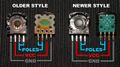
In all the boards (except sixaxis models) there are 2 small components to controll the vibration motors (small and big motors, usually labeled as SM and BM). All them seems to be manufactured by http://www.keccorp.com/
- 3 pins (transistors ?)
- 5 pins (voltage regulators ?)
- In V3.5X, VX3, VX4, VX5, VX6 ... first time the components are marked as KEX
- In VX7 and VX8 are marked as KE4 (one is Q3... the other is not labeled)

Sensors
About sensors and testpoints... In a PS3 controller board (sisaxis or dualshock 3) there are 4 data lines that are the outputs of the sensors (accelerometer X, accelerometer Y, accelerometer Z, and gyroscope), that goes from the sensor itself to a resistor and then to the toshiba T6UN6EFG controller. Every one of that lines has 2 testpoint, one before and one after the resistor, the purpose of this testpoints is to meassure the raw data from the sensors and also to check the health of that resistor (seems to be critical, either because is degraded with the use, or because could be fryed suddenly), the schematic for every one of this lines is as simple as this:
sensor output -> testpoint -> resistor -> testpoint -> toshiba T6UN6EFG controller
The resistor seems to have a value of 33K (verifyed in VX4 board only) and works as a filter
When the controller is turned off is posible to meassure the value of the resistor by meassuring resistance in between the two testpoints. When the controller is working is posible to check the sensor "raw" signal by touching in the first testpoint, and the "filtered" signal by touching the second testpoint (this is what the toshiba T6UN6EFG really gets)
About sensors location in the board... The giroscope is always located at the center of the board in between the sticks and aligned with the USB connector, this is because it meassures rotations around an imaginary axis located in that position (vertically in your room from floor to roof and passing exactly in between your controller sticks). The accelerometer is always located in the left-top corner of the board, this seems to be because this area is more sensitive for right handed people (if you are right handed and shake it with only right hand... the left side of the board is going to suffer more g-force)
- Some interesting links
Accelerometers
Hokuriku HDK 325A and 325B


https://www.hdk.co.jp/japanese/topics_j/tpc053_j.htm
Hokuriku HDK HAAM 325A and 325B
Accelerometer - 3-Axis
- Note in the photo of 325A the pins numbers are marked, and are in clockwise direction (inversed), the table below follows this clockwise order
| Pin | Name | Notes |
|---|---|---|
| 1 | GND ? | |
| 2 | V_SENSORS ? | |
| 3 | N/C ? | |
| 4 | N/C ? | |
| 5 | N/C ? | |
| 6 | ||
| 7 | ||
| 8 | SENSOR_ACCL_ ? | To Toshiba T6UN*EFG, pin ? |
| 9 | SENSOR_ACCL_ ? | To Toshiba T6UN*EFG, pin ? |
| 10 | SENSOR_ACCL_ ? | To Toshiba T6UN*EFG, pin ? |
Analog Devices 330K

16 pins. Used in board MSU_PP4.0 9 only
- Analog Devices ADXL330KCPZ, 3-Axis Accelerometer, ±3g, 1.8 → 3.6 V, LFCSP 16-Pin
- http://www.analog.com/en/products/mems/accelerometers.html
- http://uk.rs-online.com/web/c/semiconductors/sensor-ics/accelerometer-ics/?applied-dimensions=4294967128
- http://uk.rs-online.com/web/p/accelerometer-ics/0412775/
- http://docs-europe.electrocomponents.com/webdocs/0aa7/0900766b80aa75b6.pdf
| Pin | Name | Notes |
|---|---|---|
| 1 | N/C | Not connected |
| 2 | Self Test | It cant be seen in the photos but most probably this function is disabled |
| 3 | GND | To ground |
| 4 | N/C | Not connected |
| 5 | GND | To ground |
| 6 | GND | |
| 7 | GND | |
| 8 | SENSOR_ACCL_Z | To a testpoint, then resistor and capacitor to ground, then to another testpoint, then to Toshiba T6UN6EFG, pin ? |
| 9 | N/C | Not connected |
| 10 | SENSOR_ACCL_Y | To a testpoint, then resistor and capacitor to ground, then to another testpoint, then to Toshiba T6UN6EFG, pin ? |
| 11 | N/C | Not connected |
| 12 | SENSOR_ACCL_X | To a testpoint, then resistor and capacitor to ground, then to another testpoint, then to Toshiba T6UN6EFG, pin ? |
| 13 | N/C | Not connected |
| 14 | V_SENSORS | To sensors power rail |
| 15 | V_SENSORS | |
| 16 | N/C | Not connected |
Kionix KXPC4 and KXSC4


DFN
Accelerometer - 3-Axis
The pinout is the same than the Kionix KXSC4 used in Move Motion Controller
Kionix KXSC4 is used in Dualshock 3 MSU_V3.5X boards and Move Motion Controller. Same pinout than the kionix KXPC4
The boards where is used this components has solder points ready to replace it by a 32S3 Accelerometer. Are different components (probably from different manufactures) but the copper traces in the dualshock boards are connected "pin by pin" in between them
| Pin | Name | Notes |
|---|---|---|
| 1 | GND | To ground |
| 2 | N/C | Not connected |
| 3 | N/C | |
| 4 | V_SENSORS | 2.8V Switched. Power for accelerometer and gyroscope. and capacitor to ground. (and connected to TP12 in VX4 boards) |
| 5 | V_SENSORS | |
| 6 | GND | To ground. Self Test ("Pulled-down to GND" = normal operation. "Pulled-up to VDD" = self-test mode) |
| 7 | V_SENSORS | 2.8V Switched. Power for accelerometer and gyroscope. and capacitor to ground. (and connected to TP12 in VX4 boards) |
| 8 | SENSOR_ACCL_X | To a testpoint (TP33 in VX4 boards), then 33K resistor and capacitor to ground, then to another testpoint (TP36 in VX4 boards), then to Toshiba T6UN6EFG, pin 6 |
| 9 | SENSOR_ACCL_Y | To a testpoint (TP32 in VX4 boards), then 33K resistor and capacitor to ground, then to another testpoint (TP35 in VX4 boards), then to Toshiba T6UN6EFG, pin 7 |
| 10 | SENSOR_ACCL_Z | To a testpoint (TP34 in VX4 boards), then 33K resistor and capacitor to ground, then to another testpoint (TP37 in VX4 boards), then to Toshiba T6UN6EFG, pin 8 |
| 11 | GND | To ground |
| 12 | N/C | Not connected |
| 13 | N/C | |
| 14 | GND | To ground |
Unknown 14 pins

Only used in VX3_0.07 and VX3_0.08 board models (not on VX3_0.11). There is no available photo of this component because is not present in the wiki photos of the board models where it was used (and it was not posible to find it searching in google photos). By looking at the solder pads it can be seen it has the same package than the STMicroelectronics 32S3 but a different pinout
| Pin | Name | Notes |
|---|---|---|
| 1 | N/C ? | |
| 2 | SENSOR_ACCL_ ? | To Toshiba T6UN6EFG, pin ? |
| 3 | SENSOR_ACCL_ ? | To Toshiba T6UN6EFG, pin ? |
| 4 | SENSOR_ACCL_ ? | To Toshiba T6UN6EFG, pin ? |
| 5 | GND ? | |
| 6 | V_SENSORS ? | |
| 7 | V_SENSORS ? | |
| 8 | N/C ? | |
| 9 | N/C ? | |
| 10 | GND ? | |
| 11 | N/C ? | |
| 12 | N/C ? | |
| 13 | GND ? | |
| 14 | N/C ? |
STMicroelectronics 32S3

http://www.st.com/en/mems-and-sensors/accelerometers.html
14 pins (pin numbers are painted in white in some boards). Accelerometer - 3-Axis
This component seems to be fully compatible with the KIONIX KXPC4 accelerometer, actually most boards models has solder points to mount both, the kionix and this one (the boards are "ready" for both, is at manufacturing time when they decides which component to use)
Most of the photos of the different board models here in wiki uses the kionix (and this is a coincidence)... but if you look at the photo of the other side of that same board you will see an "empty" placement for this chip instead, aligned with it, in a corner of the board. The few exceptions are the most older models
| Pin | Name | Notes |
|---|---|---|
| 1 | V_SENSORS | 2.8V Switched. Power for accelerometer and gyroscope. and capacitor to ground. (and connected to TP12 in VX4 boards) |
| 2 | V_SENSORS | |
| 3 | V_SENSORS | |
| 4 | V_SENSORS | |
| 5 | GND | To ground |
| 6 | GND | |
| 7 | SENSOR_ACCL_Y | To a testpoint (TP32 in VX4 boards), then 33K resistor and capacitor to ground, then to another testpoint (TP35 in VX4 boards), then to Toshiba T6UN6EFG, pin 7 |
| 8 | SENSOR_ACCL_X | To a testpoint (TP33 in VX4 boards), then 33K resistor and capacitor to ground, then to another testpoint (TP36 in VX4 boards), then to Toshiba T6UN6EFG, pin 6 |
| 9 | SENSOR_ACCL_Z | To a testpoint (TP34 in VX4 boards), then 33K resistor and capacitor to ground, then to another testpoint (TP37 in VX4 boards), then to Toshiba T6UN6EFG, pin 8 |
| 10 | GND | To ground |
| 11 | N/C | Not connected |
| 12 | N/C | |
| 13 | V_SENSORS | 2.8V Switched. Power for accelerometer and gyroscope. and capacitor to ground. (and connected to TP12 in VX4 boards) |
| 14 | V_SENSORS |
Gyroscopes
Murata ENC-03R

| Pin | Name | Notes |
|---|---|---|
| 1 | V_SENSORS | |
| 2 | ? | |
| 3 | SENSOR_GYRO ? | |
| 4 | GND |
Epson-Toyocom X3500Z

Epson-Toyocom XV3500CB
| Pin | Name | Notes |
|---|---|---|
| 1 | ||
| 2 | ||
| 3 | ||
| 4 | GND ? | |
| 5 | ||
| 6 | ||
| 7 | ||
| 8 | V_SENSORS ? |
STMicroelectronics Y35A

http://www.st.com/en/mems-and-sensors/gyroscopes.html
10 pins (pin numbers follows the same order than the accelerometers using the same package)
| Pin | Name | Notes |
|---|---|---|
| 1 | V_SENSORS | 2.8V Switched. Power for accelerometer and gyroscope. and capacitor to ground. (and connected to TP12 in VX4 boards) |
| 2 | GND | To ground |
| 3 | ? | To 3 small SMD components one of each color... to ground |
| 4 | GND | To ground |
| 5 | N/C ? | Not connected ? |
| 6 | SENSOR_GYRO | To a testpoint (TP41 in VX4 boards), then 33K resistor and capacitor to ground, then to another testpoint (TP40 in VX4 boards), then to Toshiba T6UN6EFG, pin 9 |
| 7 | N/C ? | Not connected ? |
| 8 | GND | To ground |
| 9 | V_SENSORS | 2.8V Switched. Power for accelerometer and gyroscope. and capacitor to ground. (and connected to TP12 in VX4 boards) |
| 10 | N/C ? | Not connected ? |
Bluetooth
http://www.alps.com/products/e/category_tuner.html
48 pins (13x19mm)
ALPS 103A

Used in boards: PP4
- Components inside ALPS 103A BT module:
- PCB = 6 layers
- Logic = SCEI/CSR CXD3262GG (BlueCore4 - External - Single Chip Bluetooth Solution, V2.0+EDR)
- CSR = Cambridge Silicon Radio (later adquired by qualcomm)
- External = It means this member of the "BlueCore4 family" uses an external memory (the 8Mb NOR chip listed below)
- http://www.iec.dk/products/csrchipsinfo.asp?id=41
- http://www.iec.dk/products/csrchipdescription.asp?C_D_Id=36
- http://www.nordfield.com/downloads/datasheets-components/BlueCore4.pdf
- https://cdn.sparkfun.com/datasheets/Wireless/Bluetooth/CSR-BC417-datasheet.pdf (BC417 external)
- http://www.czwtech.com/uploadfile/cfile/201211994421454.pdf (BC41B rom)
- https://hackaday.com/2014/05/18/firmware-for-cheap-bluetooth-modules/
- Memory = SST SST39VF800A-70-4I-M1QE (Flash - NOR, 8Mb (512k x 16), Multipurpose, 3.0V, 70nS)
- 48-Ball Very-Very-Thin-Profile, Fine-Pitch Ball Grid Array (WFBGA) 4mm x 6mm
- http://www.microchip.com/wwwproducts/en/SST39VF800A
- http://ww1.microchip.com/downloads/en/DeviceDoc/25001A.pdf
- Crystal = 26MHz
- Capacitors count = 26
- Inductors count = 2
- Resistors count = 2
- SPI
- The SPI port can be used for system debugging. It can also be used for programming the Flash memory
- The DFU boot loader must be loaded into the Flash device before the UART or USB interfaces can be used. This initial flash programming can be done via the SPI
- UART
- BlueCore4-External UART interface provides a simple mechanism for communicating with other serial devices using the RS232 protocol. Four signals are used to implement the UART function. When BlueCore4-External is connected to another digital device, UART_RX and UART_TX transfer data between the two devices. The remaining two signals, UART_CTS and UART_RTS, can be used to implement RS232 hardware flow control where both are active low indicators
- http://www.summitdata.com/blog/uart-flow-control-rtscts-necessary-proper-operation-wireless-modules/
- http://simmonmt.blogspot.com.es/2011/05/rtscts-handshaking-and-waveforms.html
ALPS 203A

Used in boards: V2
ALPS 502A
Used in "some" Wireless Keypad boards
40 pins (12x15mm)
ALPS 303A

Used in boards: V2.5, VX
ALPS 113A
Used in boards: V3.5X 1.14 only, seems to be a variant of the ALPS 413A below
ALPS 413A

Used in boards: V3.5X, VX3, VX4, and "some" Move Navigation Controller boards
The pin numbers can be seen on V3.5X boards
| Pin # | Name | Port | Description |
|---|---|---|---|
| 1 | GND_SHIELD | To ground (corner solder point for the interferences metal shield) | |
| 2 | V_BT_DETECT ? | Diode to ground, and 15K resistor to pin 3 | |
| 3 | V_BT ? | To Texas Instruments SN89062 pin 7, and to TP10 in VX4 boards | |
| 4 | GND | To ground | |
| 5 | SLAVES_RESET | To resistor network, and then to Texas Instruments SN84001 pin 2 and to Toshiba T6UN6EFG pin 11 in VX4 boards | |
| 6 | BT_UART_2 ? | To Toshiba T6UN6EFG pin 15 through resistor network | |
| 7 | BT_UART_4 ? | To Toshiba T6UN6EFG pin 17 | |
| 8 | BT_UART_1 ? | To Toshiba T6UN6EFG pin 14 through resistor | |
| 9 | BT_UART_3 ? | To Toshiba T6UN6EFG pin 16 through resistor network | |
| 10 | USB_DATA+ | USB connector through resistor (and TP3 in VX4 boards) | |
| 11 | USB_DATA- | USB connector through resistor (and TP2 in VX4 boards) | |
| 12 | GND_SHIELD | To ground (corner solder point for the interferences metal shield) | |
| 13 | GND_SHIELD | To ground (corner solder point for the interferences metal shield) | |
| 14 | BT_UNK_1 | To Toshiba T6UN6EFG pin 18 | |
| 15 | POWER_BT_UNK ? | To Texas Instruments SN89062 pin 19 | |
| 16 | POWER_BT_UNK ? | To Texas Instruments SN89062 pin 14 | |
| 17 | BT_SPI_3 ? | To debug missing connector in PP4 and V2 boards... or... TP49 in V3.5X boards... or... TP76 in VX3 boards... or unlabeled testpoint in VX4, VX5, VX6 boards | |
| 18 | BT_SPI_2 ? | To debug missing connector in PP4 and V2 boards... or... TP48 in V3.5X boards... or... TP75 in VX3 boards... or unlabeled testpoint in VX4, VX5, VX6 boards | |
| 19 | BT_SPI_4 ? | To debug missing connector in PP4 and V2 boards... or... TP50 in V3.5X boards... or... TP77 in VX3 boards... or unlabeled testpoint in VX4, VX5, VX6 boards | |
| 20 | GND_SHIELD | To ground (corner solder point for the interferences metal shield) | |
| 21 | GND_SHIELD | To ground (corner solder point for the interferences metal shield) | |
| 22 | BT_SPI_1 ? | To debug missing connector in PP4 and V2 boards... or... TP47 in V3.5X boards... or... TP74 in VX3 boards... or unlabeled testpoint in VX4, VX5, VX6 boards | |
| 23 | GND | To ground | |
| 24 | N/C ? | Not connected ? | |
| 25 | V_STBY | To Texas Instruments SN89062 pin 22 | |
| 26 | GND | To ground | |
| 27 | V_STBY | To Texas Instruments SN89062 pin 22 | |
| 28 | BT_UNK_2 | Toshiba T6UN6EFG pin 19 | |
| 29 | N/C ? | Not connected ? | |
| 30 | GND | To ground | |
| 31 | N/C ? | Not connected ? | |
| 32 | GND_SHIELD | To ground (corner solder point for the interferences metal shield) | |
| 33 | GND_SHIELD | To ground (corner solder point for the interferences metal shield) | |
| 34 | ANTENNA | Antenna | |
| 35 | GND | To ground | |
| 36 | N/C ? | Not connected ? | |
| 37 | POWER_BT_UNK ? | To Texas Instruments SN89062 pin 13 | |
| 38 | POWER_BT_UNK ? | To Texas Instruments SN89062 pin 15 | |
| 39 | N/C ? | Not connected ? | |
| 40 | GND_SHIELD | To ground (corner solder point for the interferences metal shield) | |
ALPS 503A
Used in "some" Move Motion Controller boards
48 pins (11x11mm)
ALPS 603A


Used in boards: VX5, VX6, VX7
Without knowing what is inside, just based on the size of this BT module... the logic "chip" inside probably is a bluecore4-ROM based model (or 5-ROM series), this means the flash memory is integrated inside the "chip"
The pin numbers can be seen on VX7 boards
| Pin # | Name | Description | |
|---|---|---|---|
| 1 | GND_SHIELD | To ground | |
| 2 | GND | To ground | |
| 3 | |||
| 4 | POWER_BT_UNK ? | Texas Instruments A6044A0 pin 41 | |
| 5 | |||
| 6 | |||
| 7 | |||
| 8 | GND | To ground | |
| 9 | |||
| 10 | |||
| 11 | |||
| 12 | GND_SHIELD | To ground | |
| 13 | GND_SHIELD | To ground | |
| 14 | |||
| 15 | |||
| 16 | |||
| 17 | ANTENNA | Antenna | |
| 18 | |||
| 19 | |||
| 20 | |||
| 21 | |||
| 22 | |||
| 23 | |||
| 24 | GND_SHIELD | To ground | |
| 25 | GND_SHIELD | To ground | |
| 26 | To 4x resistor network (RN4 in VX7) | ||
| 27 | GND | To ground (in VX5). Or to 4x resistor network (RN4 in VX7) | |
| 28 | To 4x resistor network (RN4 in VX7) | ||
| 29 | |||
| 30 | To 4x resistor network (RN4 in VX7) | ||
| 31 | |||
| 32 | (R10 in VX7) | ||
| 33 | |||
| 34 | USB_DATA | (R7 in VX7) | |
| 35 | USB_DATA | (R9 in VX7) | |
| 36 | GND_SHIELD | To ground | |
| 37 | GND_SHIELD | To ground | |
| 38 | |||
| 39 | GND | To ground | |
| 40 | BT_SPI_3 ? | (TP25 in VX7) | |
| 41 | BT_SPI_2 ? | (TP24 in VX7) | |
| 42 | BT_SPI_4 ? | (TP26 in VX7) | |
| 43 | BT_SPI_1 ? | (TP23 in VX7) | |
| 44 | GND | To ground | |
| 45 | |||
| 46 | |||
| 47 | GND | To ground | |
| 48 | GND_SHIELD | To ground | |
Onboard (not a module)
Cambridge Silicon Radio unknown

Used in boards: VX8 only
This version of the logic "chip" probably is pretty similar (or exactly the same) than the one used inside the previous ALPS 603A BT module, the difference is the crystal and the "chip" itself has been moved out of the "old" BT modules PCB, that BT module PCB had 6 layers in previous versions and the dualshock 3 PCB had 2 layers. To make this change posible the PCB of VX8 boards is multilayer (there are a lot of traces "hidden" connected to the BT "chip")
Ways to tell if the controller is not original
.jpg)
- The SONY logo on the top of a counterfeit controller will not be aligned correctly with a originall controller.
- Different sticker label
- Counterfeit controllers have an extra screw on the back, hidden beneath the sticker.
- The label on the back of a counterfeit controller will be paper sticker.
- The label on the back of an official controller will have a thin layer of plastic over the paper sticker, giving it a matte finish and a more protected feel.
- The paper label on the back of a counterfeit controller will not be correctly aligned with the shape of the device on the back, as it was most likely put on by hand.
- Buttons
- The center Home button on a counterfeit controller will be marginally darker than the Home button on an official controller.
- Square, Triangle, Circle, and Cross buttons will be raised higher on a counterfeit controller.
- The colors of these face buttons will be dull, compared to the bright colors of an official DualShock 3.
- Sticks
- Compared to an official controller, the seams beneath the analog sticks where the bottom and top halves of the plastic meet will be sharp.
- Leds
- The LEDs lights on the controller that signify which Player it is controlling will not be flush with the outside shell. Official controllers are relatively level all the way across. Some controllers may have minor protrusion of the LEDs, though this should not be significant.
- When you turn on a counterfeit the controller, the flashing red lights on the outside will actually shine THROUGH the casing of the device, something that would never happen on an official product.
- Syncing
- If you have consistent trouble wirelessly syncing your controller to your PS3, the device may be counterfeit.
From: http://www.ps3hax.net/showthread.php?p=574042#post574042
Homebrew
- PS Seismograph 0.2.0 from Deroad:
I have updated my homebrew to 0.2.0. now it supports all tv resolution (old versions were only for 1080p/i tv)
This is a simple Seismograph for ps3. it uses all the axis of the first controller.
[Download]http://store.brewology.com/ahomebrew.php?brewid=177
[GIT] https://github.com/wargio/PS-Seismograph
[Forum] http://www.ps3hax.net/showthread.php?t=53698
[Forum] http://psx-scene.com/forums/content/ps-seismograph-0-2-0-deroad-3121/
[Blog] http://devram0.blogspot.it/
- Others : Jjolano's PS Vibe (3.55+?), PS Vibe Move Edition Deroad( or only ps move+ps eye compatible?), MultiMan: rumble and gyroscope function?
- See also Move Motion Controller page
PC Software
for use of controller on PC
- http://forums.pcsx2.net/Thread-XInput-Wrapper-for-DS3-and-Play-com-USB-Dual-DS2-Controller
- http://www.motioninjoy.com/download
- https://www.youtube.com/watch?v=FsUtQ8urmw0
- http://betterds3.ciebiera.net/
- http://xpadder.com/
- http://www.rapiro.com/downloads/ (Sony Dualshock 3 gamepad to work in Raspberry Pi on RAPIRO)
Nefarius tools for use of controller on PC
ScpToolkit
- https://github.com/nefarius/ScpToolkit (Windows Driver and XInput Wrapper for Sony DualShock 3/4 Controllers)
- ScpToolkit XInput Wrapper aka ScpServer Reloaded on forums.pcsx2.net
FireShock
- https://github.com/nefarius/FireShock (Bluetooth is not supported yet, USB only as of 09/2017)
- FireShock on forums.pcsx2.net
- https://vigem.org/ (HIDUSB filter driver for Sony DualShock controllers)
- https://github.com/nefarius/ViGEm (Virtual Gamepad Emulation Framework)
Related Hardware
USB host adapter
- http://www.hobbytronics.co.uk/usb-host/ps3-controller Connect a PS3 Dualshock Controller to the USB Host Board
Other
- nice PCB overview of revisions: http://forums.xbox-scene.com/lofiversion/index.php/t648322.html - offline forum
- http://forums.xbox-scene.com/index.php?/topic/648322-ps3-controller-versions-and-tp-spots/ - offline forum
- http://s50.photobucket.com/user/RDCXBG/library/PS3%20Six-Axis%20and%20DS3 - RDC photobucket
- sony-ps3-controller.pdf - transcription of the (missing) RDC thread on (defunct) xbox-scene forum
| |||||||||||||