SW-302: Difference between revisions
Jump to navigation
Jump to search
mNo edit summary |
No edit summary |
||
| (2 intermediate revisions by 2 users not shown) | |||
| Line 1: | Line 1: | ||
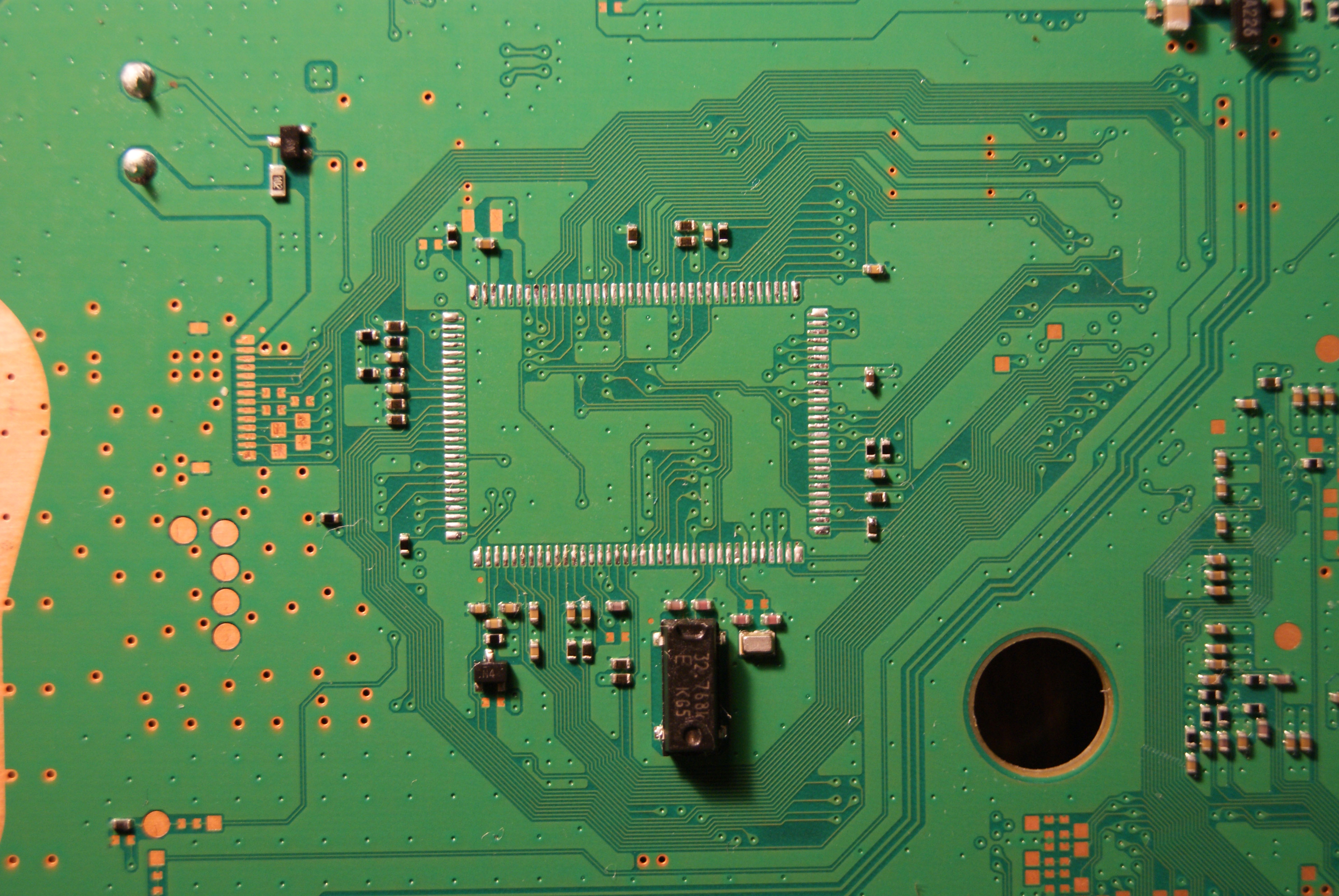
<div style="float:right">[[File:Syscon-sw302.jpg|thumb|Photo of rev2 subversion on [[CECHLxx|CECHL]]/[[VER-00x|VER-001]]<br />Syscon 'SW-302' 2-2nd Generation (QFP Packaging)]]<br /><br />[[File:Fp128b_pin_arrangement.png|thumb|QFP Package : 128 pins<br />Syscon 'SW-301' 2nd Generation<br />''pin 1 left bottom at mark, counter clockwise from south (pins 1-38) to east (pins 39-64), north (pins 65-102), west (103-128))'']]</div> | <div style="float:right">[[File:Syscon-sw302.jpg|thumb|Photo of rev2 subversion on [[CECHLxx|CECHL]]/[[VER-00x|VER-001]]<br />Syscon 'SW-302' 2-2nd Generation (QFP Packaging)]]<br /><br />[[File:Fp128b_pin_arrangement.png|thumb|QFP Package : 128 pins<br />Syscon 'SW-301' 2nd Generation<br />''pin 1 left bottom at mark, counter clockwise from south (pins 1-38) to east (pins 39-64), north (pins 65-102), west (103-128))'']]</div> | ||
*Found in PS3 models: | |||
**[[CECHLxx]] with [[VER-001]] motherboard | |||
{{Template:Syscon pinout LQFP 128 pins}} | |||
{{Motherboard Components}}<noinclude>[[Category:Main]]</noinclude> | |||
{{ | |||
[[Category: | |||
Latest revision as of 04:39, 29 January 2022


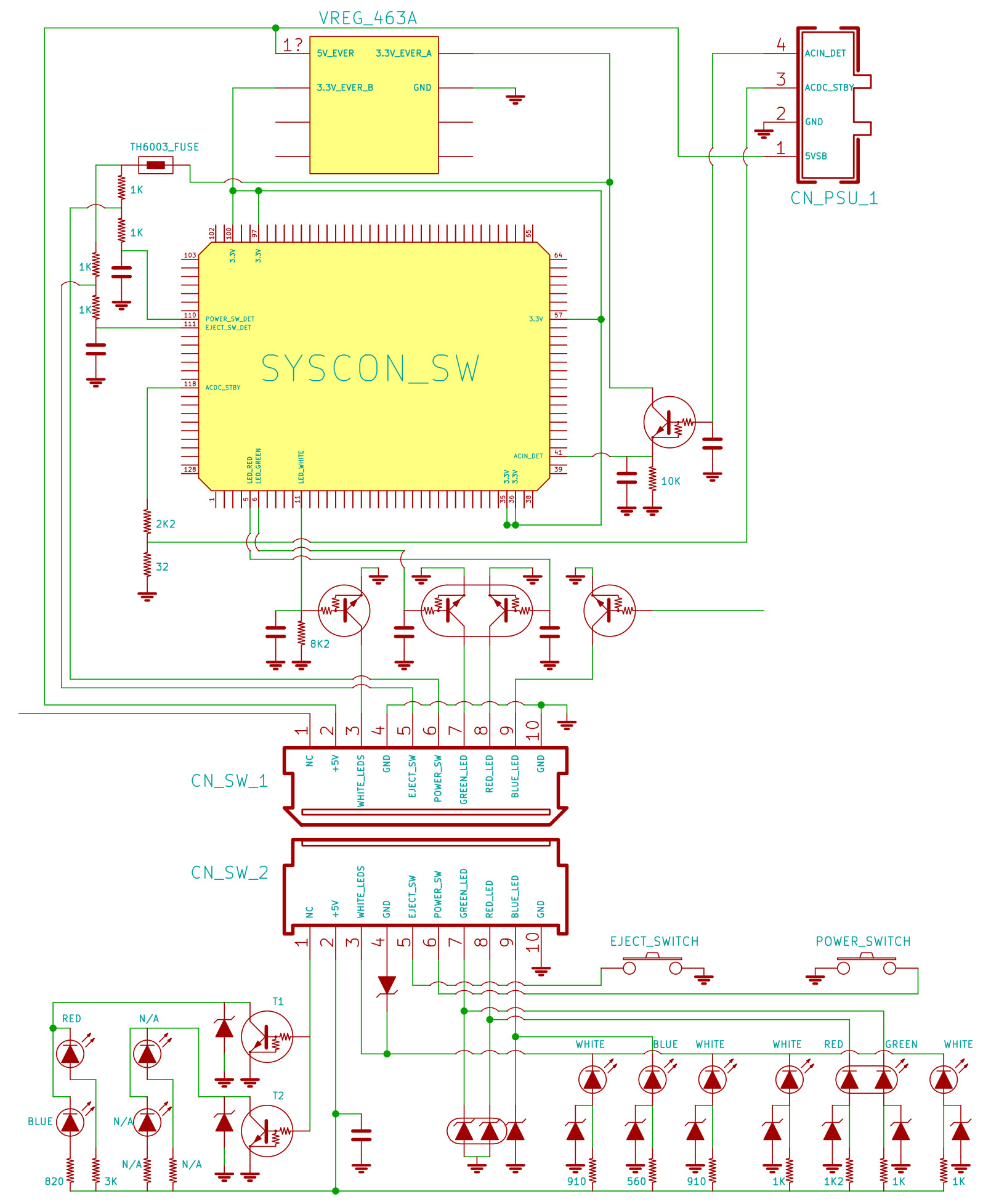
Pinout


| Pin | Port | Name | Type | Description | Voltages | |
|---|---|---|---|---|---|---|
| NEC/Renesas | Sony/Custom | |||||
| 1 | 14 | SCL20 | HDMI_I2C_SCL | Connected to HDMI controller MN8647091 pin 27 | 0 | |
| 2 | 14 | INTP7 | SB_INT/SYSCSINT | Connected to South Bridge CXD9963GB pad W22 through a resistor | ~1V @ standby (0 V?) | |
| 3 | 14 | INTP6 | BE_INT/ATTENTION | Connected to CELL pad BA17 (1342 pads layout), or pad UNK (1308 pads layout) through a NPN transistor | 3V @ standby (3.15V) | |
| 4 | 12 | EXLVI | Connected to +12V_MAIN through a resistor and divider (EXLVI config = External potential input for low-voltage detector ?) | 0 | ||
| 5 | 3 | P37 | POW_LED | Connected to Switch board dual led (Green) through a dual digital NPN transistor EMH1(SOT-563) | 0 | |
| 6 | 3 | P36 | STBY_LED | Connected to Switch board dual led (Red) through a dual digital NPN transistor EMH1(SOT-563) | 3v @ standby (3.3V) | |
| 7 | 3 | P35 | ? | Connected to South Bridge CXD9963GB pad AA18 (SB_RESET ?, or SB_CGRST ?), see talk page | 0 | |
| 8 | 3 | P34 | ? | Connected to South Bridge CXD9963GB pad AA17 (SB_RESET ?, or SB_CGRST ?), see talk page | 0 | |
| 9 | 3 | P33 | Connected to CELL pad AW18 ? (1342 pads layout), or pad UNK ? (1308 pads layout) (BE_RESET ?) | 0 | ||
| 10 | 3 | P32 | ? | 0 | ||
| 11 | 16 | TO13 | BACK_LEDS | Connected to Switch board backlit LEDs through a transistor | 0 | |
| 12 | 16 | TO12 | SW_PWM ? | Connected to Switch board contour LEDs through a transistor | 0 | |
| 13 | 16 | NOT_CONNECTED. Floating through a missing SMD component. See: NOWHERE | 0 | |||
| 14 | 16 | NOT_CONNECTED. Floating through a missing SMD component at the other side of the board. See: VIA | 0 | |||
| 15 | 4 | P47/INTP2 | Connected to HDMI controller MN8647091 pin 94 | 0 | ||
| 16 | 4 | TO05 | BUZZER | Connected to the Buzzer through a transistor | 0 | |
| 17 | 4 | SO01 | Connected to South Bridge CXD9963GB pad UNK ? (SB_SPI_DO ?) / CELL pad AV13 (1308 pads layout, BE_SPI_DO) | 0 | ||
| 18 | 4 | SI01 | Connected to South Bridge CXD9963GB pad UNK ? (SB_SPI_DI ?) / CELL pad BA13 (1308 pads layout, BE_SPI_DI) | 3v @ standby | ||
| 19 | 4 | SCK01 | Connected to South Bridge CXD9963GB pad UNK ? (SB_SPI_CLK ?) / CELL pad AY13 (1308 pads layout, BE_SPI_CLK) | 0 | ||
| 20 | 4 | P42 | Connected to South Bridge CXD9963GB pad UNK ? (SB_SPI_CS ?) / CELL pad AW13 (1308 pads layout, BE_SPI_CS) | 0 | ||
| 21 | 4 | TOOL1 | TOOL_CLK | Connected to Service Connector 3rd Gen. pin 13 (Tool clock) through a missing resistor | 3.0 | |
| 22 | 4 | TOOL0 | TOOL_DAT | Connected to Service Connector 3rd Gen. pin 7 (Tool Data) through a missing resistor | 0 | |
| 23 | 12 | P127 | ? | 0 | ||
| 24 | 12 | SDA21 | THR_I2C_SDA | Connected to Temperature Monitors pin 7 (SMBus data) | 3v @ standby (3.15) | |
| 25 | 12 | SCL21 | THR_I2C_SCL | Connected to Temperature Monitors pin 8 (SMBus clock) | 3v @ standby (3.15) | |
| 26 | RESET | RST | Connected to Service Connector 3rd Gen. pin 9 through a missing resistor Connected to standby voltage regulator Mitsumi 463A pin 3 |
|||
| 27 | 12 | XT2 | OSCOUT | Connected to a crystal (Subsystem clock). CLK -> 1-2V Amplitude (32.768Khz) | ||
| 28 | 12 | XT1 | OSCIN | Connected to a crystal (Subsystem clock). CLK -> 1-2V Amplitude (32.768Khz) | ||
| 29 | FLMD0 | FLASH_MODE | Connected to Service Connector 3rd Gen. pin 8 (Flash programming mode) through a missing resistor | 3.33 | ||
| 30 | 12 | X2 | XTAL | Connected to a crystal (Main system clock) marked "EX" (16.9344Mhz?) | 0.8v @ standby (1.1) | |
| 31 | 12 | X1 | EXTAL | Connected to a crystal (Main system clock) marked "EX" (16.9344Mhz?) | 2.2v @ standby (2.4) | |
| 32 | REGC | VDDbat | Connected to battery+ through 2 diodes Connected to a capacitor (internal voltage regulator, around 1uF) at the other side of the board. See: VIA |
|||
| 33 | VSS0 | GND | 0 | |||
| 34 | EVSS0 | GND | 0 | |||
| 35 | VDD | 3.3_EVER_B | Connected to standby voltage regulator Mitsumi 463A pin 2 | 3v @ standby (3.3) | ||
| 36 | EVDD0 | 3.3_EVER_B | Connected to standby voltage regulator Mitsumi 463A pin 2 | 3v @ standby (3.3) | ||
| 37 | 6 | SCL0 | MK_I2C_SCL | Connected to Texas Instruments-SCEI Clock Generator CDC972 pin 37 | 0.2v @ standby | |
| 38 | 6 | SDA0 | MK_I2C_SDA | Connected to Texas Instruments-SCEI Clock Generator CDC972 pin 38 | 0.2v @ standby | |
| 39 | 6 | P62 | ? | 0 | ||
| 40 | 6 | P63 | P63_DOWN | 10K resistor to GND | 0 | |
| 41 | 3 | INTP4 | ACIN_DET | Connected to Power Supply control connector pin 4 through a transistor. See: schematic | 3v @ standby (3.3) | |
| 42 | 6 | P64/RD | Connected to voltage regulator BD9684 0906 pin 4 (enable something) through some undocumented components | 0 | ||
| 43 | 6 | WR0 | ? | Connected to Service Connector 3rd Gen. pin 12 through a missing resistor | 3.0 | |
| 44 | 6 | P66/WR1 | ? | 0 | ||
| 45 | 6 | NOT_CONNECTED. | 0 | |||
| 46 | 7 | P77/EX23/KR7/INTP11 | Connected to CELL pad BA19 ? (1342 pads layout), or pad UNK (1308 pads layout) through a transistor (labeled 26 and located near the CELL temperature monitor) (inverted direction than the signal from pin 109) BE_POWGOOD ? |
0 | ||
| 47 | 7 | P76/EX22/KR6/INTP10 | ? | 3v @ standby (3.15) | ||
| 48 | 7 | INTP9 | VD_VINT0/RSX_VINTE0 | Connected to RSX pad AR22 (41x41 layout) through a transistor | 3v @ standby (3.15) | |
| 49 | 7 | P74 |
P74_DOWN | 10K resistor to GND | 0 | |
| 50 | 7 | KR3 | ? | Connected to Service Connector 3rd Gen. pin 3 Connected to voltage regulator D35653 0S25 (FLASH_ENABLE ?) |
0 | |
| 51 | 7 | P72/EX18/KR2 | ? | Connected to xxxxxxxxxxxxxx through transistor | 0 | |
| 52 | 7 | P71/EX17/KR1 | Connected to voltage regulator Rohm BD3525 pin 12 (enable something) | 0 | ||
| 53 | 7 | P70/EX16/KR0 | ? | 0 | ||
| 54 | 0 | P06 |
P06_DOWN | 45K resistor array to GND | 0 | |
| 55 | 0 | P05 |
P05_DOWN | 45K resistor array to GND | 0 | |
| 56 | EVSS1 | GND | 0 | |||
| 57 | EVDD1 | 3.3_EVER_B | Connected to standby voltage regulator Mitsumi 463A pin 2 | 3v @ standby (3.3) | ||
| 58 | 8 | P80/EX0 | ? | 47k resistor tied to vcc | 0 | |
| 59 | 8 | P81/EX1 | ? | 47k resistor tied to vcc | 0 | |
| 60 | 8 | P82/EX2 | ? | 47k resistor tied to vcc | 0 | |
| 61 | 8 | P83/EX3 | ? | 47k resistor tied to vcc | 0 | |
| 62 | 8 | P84/EX4 | ? | 47k resistor tied to vcc | 0 | |
| 63 | 8 | P85/EX5 | ? | 47k resistor tied to vcc | 0 | |
| 64 | 8 | P86/EX6 | ? | 47k resistor tied to vcc | 0 | |
| 65 | 8 | P87/EX7 | ? | tied to a resistor of 10k | 0 | |
| 66 | 3 | P30/INTP3/RTC1HZ | ? | goes to isl 6325 pin 9 | 0 | |
| 67 | 5 | P50/EX8 | ? | goes to isl 6325 pin 8 | 0 | |
| 68 | 5 | P51/EX9 | ? | goes to isl 6325 pin 7 | 0 | |
| 69 | 5 | P52/EX10 | ? | goes to isl 6325 pin 6 | 0 | |
| 70 | 5 | P53/EX11 | ? | goes to isl 6325 pin 5 | 0 | |
| 71 | 5 | P54/EX12 | ? | goes to isl 6325 pin 4 | 0 | |
| 72 | 5 | P55/EX13 | ? | goes to isl 6325 pin 3 | 0 | |
| 73 | 5 | P56/EX14 | ? | goes to isl 6325 pin 2 | 0 | |
| 74 | 5 | P57/EX15 | ? | goes to isl 6325 pin 20 | 0 | |
| 75 | 1 | RSX_VDDR_EN | Connected to RSX through voltage regulator Mitsumi 810X pin 5 | 0 | ||
| 76 | 1 | INTP5 | RSX_INT | Connected to RSX pad AY7 (41x41 layout) through a transistor | 3v @ standby (3.15) | |
| 77 | 1 | P15/EX29/RTCDIV/RTCCL | ? | 3v @ standby (3.3) | ||
| 78 | 1 | RxD3 | UART0_RxD | Connected to Service Connector 3rd Gen. pin 11 (UART-TTL terminal Receive) through a missing resistor Connected to PCI Connector pin 6 |
0 | |
| 79 | 1 | TxD3 | UART0_TxD | Connected to Service Connector 3rd Gen. pin 10 (UART-TTL terminal Transmit) through a missing resistor Connected to PCI Connector pin 4 |
3.3 | |
| 80 | 1 | SO00 | BE_SPI_DO / SB_SPI_DO | Connected to CELL pad AV13 (1342 pads layout) / South Bridge pad V19 CXD9963GB. Serial Output from Syscon Master to Cell/SB Slave (MOSI) | 0 | |
| 81 | 1 | SI00 | BE_SPI_DI / SB_SPI_DI | Connected to CELL pad BA13 (1342 pads layout) / South Bridge pad V22 CXD9963GB. Serial Input from Cell/SB Slave to Syscon Master (MISO) | 1.2 | |
| 82 | 1 | SCK00 | BE_SPI_CLK / SB_SPI_CLK | Connected to CELL pad AY13 (1342 pads layout) / South Bridge pad U18 CXD9963GB. 2.5 Mhz SPI Clock | ||
| 83 | 9 | P90 | BE_SPI_CS / SB_SPI_CS | Connected to CELL pad AW13 (1342 pads layout) / South Bridge pad U19 CXD9963GB. Chip Select | 2.0 | |
| 84 | 9 | P91/EX33 | ? | 3v @ standby | ||
| 85 | 9 | P92/EX34 | ? | 0 | ||
| 86 | 9 | P93/EX35 | ? | 0 | ||
| 87 | 9 | P94 | Connected to RSX pad AW8 ? (41x41 layout) (RSX_SPI_CS ?) | 0 | ||
| 88 | 9 | SCK11 | Connected to RSX pad AY8 ? (41x41 layout) (RSX_SPI_CLK ?) | 0 | ||
| 89 | 9 | SI11 | Connected to RSX pad BA7 ? (41x41 layout) (RSX_SPI_DI ?) | 0 | ||
| 90 | 9 | SO11 | Connected to RSX pad BA6 ? (41x41 layout) (RSX_SPI_DO ?) | 0 | ||
| 91 | 11 | P112 | ? | 0 | ||
| 92 | 11 | P113 | Connected to voltage regulator BD3527 pin 12 (located near FLASH) | 0 | ||
| 93 | 11 | P114 | ? | goes to BD352 ic pin 12 | 0 | |
| 94 | 11 | P115 | ? | Connected to xxxxxxxxxxxxxx through transistor / BD949 pin 5 | 0 | |
| 95 | 11 | P116 | Connected to voltage regulator BD3527 pin 12 (located near USB) | 0 | ||
| 96 | 11 | P117 | AV_EN | Connected to MultiAV connector pin 3 (+5V output) through a transistor | 0 | |
| 97 | AVREF1 | 3.3_EVER_B | Connected to standby voltage regulator Mitsumi 463A pin 2 | 3v @ standby (3.3) | ||
| 98 | 11 | NOT_CONNECTED. | 0 | |||
| 99 | 11 | NOT_CONNECTED. | 0 | |||
| 100 | AVREF0 | 3.3_EVER_B | Connected to standby voltage regulator Mitsumi 463A pin 2 | 3v @ standby (3.3) | ||
| 101 | AVSS0 | GND | 0 | |||
| 102 | 15 | P157 |
P157_DOWN | 100k resistor to GND. And to a missing SMD component to VIA to pin 8 of voltage regulator Mitsumi 463A (3.3_EVER_A) | 0 | |
| 103 | 15 | ANI14_UP | VIA to 100k resistor to pin 8 of voltage regulator Mitsumi 463A (3.3_EVER_A) | 0 | ||
| 104 | 15 | ANI13_DOWN | VIA to 100k resistor to GND | 0 | ||
| 105 | 15 | 100k resistor to GND | 0 | |||
| 106 | 15 | 100k resistor to GND | 0 | |||
| 107 | 15 | on cell front transistor | 0 | |||
| 108 | 15 | pass on 100 ohms resistance then to power front panel | 0 | |||
| 109 | 15 | THERMAL_OVERLOAD ? | Connected to CELL pad AV23 ? (1342 pads layout), or pad UNK (1308 pads layout) through a transistor (labeled ND and located near the CELL temperature monitor) (inverted direction than the signal from pin 46) SYS_THR_ALRT ? And to 10k resistor to VIA to pin 8 of voltage regulator Mitsumi 463A (3.3_EVER_A) |
3v @ standby | ||
| 110 | 2 | POW_SW | Connected to Switch board power switch | 3v @ standby (3.3) 3.3 | ||
| 111 | 2 | EJECT_SW | Connected to Switch board eject switch | 3v @ standby (3.3) 3.3 | ||
| 112 | 2 | P25/ANI5 | ? | Connected to Wifi/BT module (BT_WAKEON/BT_WAKE ? (input), BT_RESET ? (output), or WLAN_RESET/11G_RESET ? (output)) | 0 | |
| 113 | 2 | P24/ANI4 | ? | Connected to Wifi/BT module (BT_WAKEON/BT_WAKE ? (input), BT_RESET ? (output), or WLAN_RESET/11G_RESET ? (output)) | 0 | |
| 114 | 2 | P23/ANI3 | ? | to resistance 55 ohms to bdrom pin 11 | 0 | |
| 115 | 2 | Connected to Bluray Drive 8-pins connector pin 8 through 100ohm resistor (DISC_CHUCK or DISC_OUT8_SW or DISC_OUT12_SW or |
0 | |||
| 116 | 2 | Connected to Bluray Drive 8-pins connector pin 7 through 100ohm resistor (DISC_CHUCK or DISC_OUT8_SW or DISC_OUT12_SW or |
0 | |||
| 117 | 2 | Connected to Bluray Drive 8-pins connector pin 6 through 100ohm resistor (DISC_CHUCK or DISC_OUT8_SW or DISC_OUT12_SW or |
(0V?) | |||
| 118 | 13 | P130 | ACDC_STBY | Connected to Power Supply control connector pin 3 through a 2K2ohm resistor. See: schematic | 3v @ standby (3.3) | |
| 119 | 13 | P131 |
HDMI_EN | Connected to voltage regulator Mitsumi 348A pins 2 and 7 Connected to HDMI connector pin 18 (+5V_ANA ?) through a transistor |
3v @ standby (3.3) | |
| 120 | 0 | P07 | ? | Connected to HDMI controller MN8647091 pin 95 through 3.6K resitor | 0 | |
| 121 | 0 | SCL10 | DVE_I2C_SCL | Connected to Digital Video Encoder CXM4027R pin 35 | 0 | |
| 122 | 0 | SDA10 | DVE_I2C_SDA | Connected to Digital Video Encoder CXM4027R pin 36 | 0 | |
| 123 | 0 | P02 | ? | to pin 12 bdrom port (DISC_IN or DISC_PHOT_LED ?) | 0 | |
| 124 | 0 | P01/TO00 | ? | Connected to HDMI controller MN8647091 pin 93 | 0 | |
| 125 | 0 | P00/TI00 | ? | to bottom transistor under optical port | 0 | |
| 126 | 14 | TO07 | FANPWM0 | Connected to the FAN grey wire (PWM duty) | 0 | |
| 127 | 14 | P144 | ? | to pin 17 bdrom port (DISC_IN or DISC_PHOT_LED ?) | 0 | |
| 128 | 14 | SDA20 | HDMI_I2C_SDA | Connected to HDMI controller MN8647091 pin 29 | 0 | |
| |||||||||||||||||||||||||||||||||||||||||||||||||||||||||||||||||||||||||||||||||||||||||||||||||||||||||||||||||||||||||||||||||||||||||||||||||||||||||||||||||||||||||||||
