Syscon Hardware: Difference between revisions
Jump to navigation
Jump to search
No edit summary |
|||
| Line 1: | Line 1: | ||
== General Information == | |||
== Topside Pinout == | Syscon is the main power controller chip. It is responsible for powering up the various power systems and for configuring and initialising the CELL, RSX and southbridge. It communicates with these devices via seperate SPI busses. There is external access by JTAG (Which appears to have been disabled after factory programming) and Serial. | ||
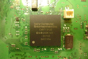
== Generation 1 == | |||
[[File:SYSCON_GEN1.JPG|thumb|Syscon 1st Generation (BGA Packaging)]] | |||
BGA Package : 200 Pins | |||
Pin's are labelled in the service manual for this generation | |||
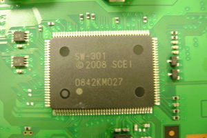
== Generation 2 == | |||
[[File:SYSCON_GEN2.JPG|thumb|Syscon 2nd Generation (QFP Packaging)]] | |||
QFP Package : 128 pins | |||
Currently there is no known pin labelling for this generation | |||
== CECHG02 Pinout == | |||
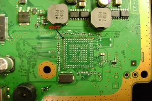
=== Topside Pinout === | |||
[[File:syscon_top.jpg|thumbnail|Syscon Top Pinouts]] | [[File:syscon_top.jpg|thumbnail|Syscon Top Pinouts]] | ||
{| | {|class="wikitable" | ||
! Pin # | ! Pin # | ||
! Name | ! Name | ||
| Line 62: | Line 79: | ||
|} | |} | ||
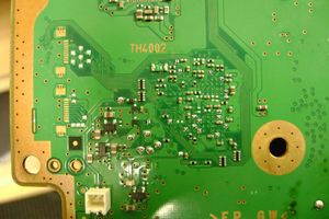
== Bottomside Pinout == | === Bottomside Pinout === | ||
[[File:syscon_bottom.jpg|thumbnail|Syscon Bottom Pinouts]] | [[File:syscon_bottom.jpg|thumbnail|Syscon Bottom Pinouts]] | ||
{| | {|class="wikitable" | ||
! Pin # | ! Pin # | ||
! Name | ! Name | ||
| Line 158: | Line 175: | ||
|Unknown | |Unknown | ||
|} | |} | ||
Revision as of 02:52, 8 April 2011
General Information
Syscon is the main power controller chip. It is responsible for powering up the various power systems and for configuring and initialising the CELL, RSX and southbridge. It communicates with these devices via seperate SPI busses. There is external access by JTAG (Which appears to have been disabled after factory programming) and Serial.
Generation 1
BGA Package : 200 Pins
Pin's are labelled in the service manual for this generation
Generation 2
QFP Package : 128 pins
Currently there is no known pin labelling for this generation
CECHG02 Pinout
Topside Pinout
| Pin # | Name | Description |
|---|---|---|
| B3 | SW_10 | Unknown |
| A6 | MC_RESERVED2 | Unknown |
| E10 | MUL_CHKSTP_OUT | Unknown |
| C15 | VSS | Power Ground |
| B16 | OSCOUT | Goes to unpopulated crystal |
| C16 | OSCIN | From unpupulated crystal |
| B15 | POW_FAIL | Power Failure Signal |
| H1 | PN5 | Unknown |
| H2 | PN6 | Unknown |
| R1 | PM7 | Unknown |
| R2 | PM6 | Unknown |
| M4 | SW9 | Unknown |
| M10 | XDR_FET_SCK | Unknown |
Bottomside Pinout
| Pin # | Name | Description |
|---|---|---|
| R5 | VDD | +3.3v |
| R7 | DVDD | +1.8v |
| C15 | VSS | Power Ground |
| N16 | DIAG_MODE | Unknown |
| N15 | BACKUP_MODE | Unknown |
| P16 | UART0_TxD | Serial |
| P15 | UART0_RxD | Serial |
| R9 | PQ1 | Unknown |
| B12 | POW_SW | Power Switch |
| A12 | EJECT_SW | Eject Switch |
| L7 | JNTAST | JTAG |
| L8 | JRTCK | JTAG |
| L9 | JTMS | JTAG |
| K7 | JTDI | JTAG |
| K8 | JTCK | JTAG |
| K9 | JTDO | JTAG |
| M6 | SW_7_B | Unknown |
| M8 | FANPWM1 | Unknown |
| E5 | GX_VSRT | Unknown |
| B5 | DVE_RST | Unknown |
| G4 | HDMI_RST1 | Unknown |
| D4 | XDR_FET_RST | Unknown |


