Template:Syscon pinout LQFP 128 pins: Difference between revisions
Jump to navigation
Jump to search
m (Height unlocked (only here)) |
m (Added column for ports info) |
||
| Line 6: | Line 6: | ||
<includeonly><div style="height:1400px; overflow:auto"></includeonly> | <includeonly><div style="height:1400px; overflow:auto"></includeonly> | ||
{|class="wikitable mw-datatable" | {|class="wikitable mw-datatable" | ||
! rowspan="2" | Pin # !! colspan="2" | Name !! rowspan="2" | Type !! rowspan="2" | Description !! rowspan="2" | STBY Voltages | ! rowspan="2" | Pin# !! rowspan="2" | Port !! colspan="2" | Name !! rowspan="2" | Type !! rowspan="2" | Description !! rowspan="2" | STBY Voltages | ||
|- | |- | ||
! <abbr title="NEC/Renesas optional pin configuration">NEC/Renesas</abbr> !! Sony/Custom | ! <abbr title="NEC/Renesas optional pin configuration">NEC/Renesas</abbr> !! Sony/Custom | ||
|+ Syscon pinout LQFP 128 pins <span class="plainlinks" style="font-size:80%; float:right;">[ [[Template_talk:Syscon_pinout_LQFP_128_pins|Discuss]] ] or [ [{{fullurl:Template:Syscon_pinout_LQFP_128_pins|action=edit}} Edit] ]</span> | |+ Syscon pinout LQFP 128 pins <span class="plainlinks" style="font-size:80%; float:right;">[ [[Template_talk:Syscon_pinout_LQFP_128_pins|Discuss]] ] or [ [{{fullurl:Template:Syscon_pinout_LQFP_128_pins|action=edit}} Edit] ]</span> | ||
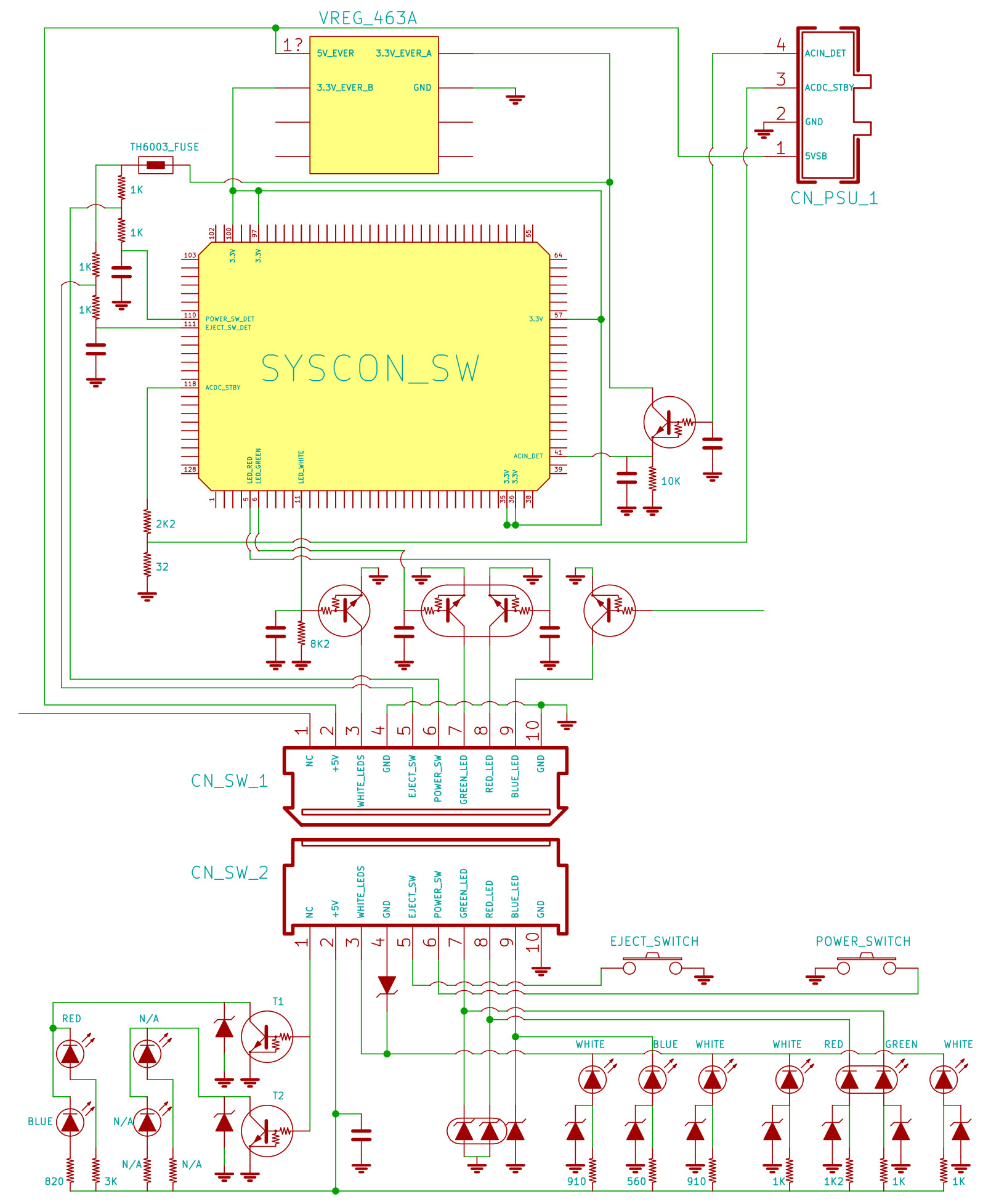
| 1 || P142/<span style="text-decoration: overline;">SCK20</span>/SCL20 || || ←I || Connected to pin27 @Panasonic [[MN8647091]] (HDMI controller CEC data channel related with pins 127 and 128 ?) || 0 | | 1 || || P142/<span style="text-decoration: overline;">SCK20</span>/SCL20 || || ←I || Connected to pin27 @Panasonic [[MN8647091]] (HDMI controller CEC data channel related with pins 127 and 128 ?) || 0 | ||
|- | |- | ||
| 2 || <s>P141/PCLBUZ1/</s>INTP7 || SB_INT/SYSCSINT || ←I || Connected to pinD1@SB [[CXD9963GB]] through the resistor || ~1V @ standby (0 V?) | | 2 || || <s>P141/PCLBUZ1/</s>INTP7 || SB_INT/SYSCSINT || ←I || Connected to pinD1@SB [[CXD9963GB]] through the resistor || ~1V @ standby (0 V?) | ||
|- | |- | ||
| 3 || <s>P140/PCLBUZ0/</s>INTP6 || BE_INT/ATTENTION || ←I || Connected to pinBA17@[[CELL BE|BE]] through the NPN transistor (CELL switches the transistor to connect this pin to GND) || 3V @ standby (3.15V) | | 3 || || <s>P140/PCLBUZ0/</s>INTP6 || BE_INT/ATTENTION || ←I || Connected to pinBA17@[[CELL BE|BE]] through the NPN transistor (CELL switches the transistor to connect this pin to GND) || 3V @ standby (3.15V) | ||
|- | |- | ||
| 4 || P120/INTP0/EXLVI || || ←I/O→ || To +12V_MAIN through the resistor and divider (EXLVI config = External potential input for low-voltage detector ?) || 0 | | 4 || || P120/INTP0/EXLVI || || ←I/O→ || To +12V_MAIN through the resistor and divider (EXLVI config = External potential input for low-voltage detector ?) || 0 | ||
|- | |- | ||
| 5 || {{cellcolors|#d699ff}} P37 || POW_LED || O→ || Connected to dual led(Green) on [[switch boards|Switch board]] through the dual digital NPN trans. EMH1(SOT-563) || 0 | | 5 || || {{cellcolors|#d699ff}} P37 || POW_LED || O→ || Connected to dual led(Green) on [[switch boards|Switch board]] through the dual digital NPN trans. EMH1(SOT-563) || 0 | ||
|- | |- | ||
| 6 || {{cellcolors|#d699ff}} P36 || STBY_LED || O→ || Connected to dual led(Red) on [[switch boards|Switch board]] through the dual digital NPN trans. EMH1(SOT-563) || 3v @ standby (3.3V) | | 6 || || {{cellcolors|#d699ff}} P36 || STBY_LED || O→ || Connected to dual led(Red) on [[switch boards|Switch board]] through the dual digital NPN trans. EMH1(SOT-563) || 3v @ standby (3.3V) | ||
|- | |- | ||
| 7 || P35 || || ←I/O→ || Connected to pinAA18@SB [[CXD9963GB]] || 0 | | 7 || || P35 || || ←I/O→ || Connected to pinAA18@SB [[CXD9963GB]] || 0 | ||
|- | |- | ||
| 8 || P34 || || ←I/O→ || Connected to pinAA17@SB [[CXD9963GB]] || 0 | | 8 || || P34 || || ←I/O→ || Connected to pinAA17@SB [[CXD9963GB]] || 0 | ||
|- | |- | ||
| 9 || P33 || || ←I/O→ || CELL BE related? || 0 | | 9 || || P33 || || ←I/O→ || CELL BE related? || 0 | ||
|- | |- | ||
| 10 || P32 || || ←I/O→ || || 0 | | 10 || || P32 || || ←I/O→ || || 0 | ||
|- | |- | ||
| 11 || {{cellcolors|#d699ff}} <s>P163/TI13/</s>TO13 || BACK_LEDS || O→ || Connected to Backlit LEDs on [[switch boards|Switch board]] || 0 | | 11 || || {{cellcolors|#d699ff}} <s>P163/TI13/</s>TO13 || BACK_LEDS || O→ || Connected to Backlit LEDs on [[switch boards|Switch board]] || 0 | ||
|- | |- | ||
| 12 || {{cellcolors|#d699ff}} <s>P162/TI12/</s>TO12 || CONTOUR_LEDS || O→ || Connected to CONTOUR LEDs on [[switch boards|Switch board]] || 0 | | 12 || || {{cellcolors|#d699ff}} <s>P162/TI12/</s>TO12 || CONTOUR_LEDS || O→ || Connected to CONTOUR LEDs on [[switch boards|Switch board]] || 0 | ||
|- | |- | ||
| 13 || {{cellcolors|#e0e0e0}} <s>P161/TI11/TO11</s> || NOT_CONNECTED || - || Disconnected to GND through a missing SMD component. See: [[Media:Syscon_SW2-303_Unsoldered.JPG|NOWHERE]] || 0 | | 13 || || {{cellcolors|#e0e0e0}} <s>P161/TI11/TO11</s> || NOT_CONNECTED || - || Disconnected to GND through a missing SMD component. See: [[Media:Syscon_SW2-303_Unsoldered.JPG|NOWHERE]] || 0 | ||
|- | |- | ||
| 14 || {{cellcolors|#e0e0e0}} <s>P160/TI10/TO10</s> || NOT_CONNECTED || - || Disconnected to GND through a missing SMD component at the other side of the board. See: [[Media:Syscon_SW2-303_Unsoldered.JPG|VIA]] || 0 | | 14 || || {{cellcolors|#e0e0e0}} <s>P160/TI10/TO10</s> || NOT_CONNECTED || - || Disconnected to GND through a missing SMD component at the other side of the board. See: [[Media:Syscon_SW2-303_Unsoldered.JPG|VIA]] || 0 | ||
|- | |- | ||
| 15 || P47/INTP2 || || ←I/O→ || Unknown purpose. The trace goes in the direction of the Wifi/BT module || 0 | | 15 || || P47/INTP2 || || ←I/O→ || Unknown purpose. The trace goes in the direction of the Wifi/BT module || 0 | ||
|- | |- | ||
| 16 || {{cellcolors|#123456|#ffffff}} <s>P46/INTP1/TI05/</s>TO05 || BUZZER || O→ || Connected to the base of a transistor that drives a pin of the buzzer to GND || 0 | | 16 || || {{cellcolors|#123456|#ffffff}} <s>P46/INTP1/TI05/</s>TO05 || BUZZER || O→ || Connected to the base of a transistor that drives a pin of the buzzer to GND || 0 | ||
|- | |- | ||
| 17 || P45/SO01 || || ←I/O→ || SB_SPI_DO @[[CXD9963GB]] ? || 0 | | 17 || || P45/SO01 || || ←I/O→ || SB_SPI_DO @[[CXD9963GB]] ? || 0 | ||
|- | |- | ||
| 18 || P44/SI01 || || ←I/O→ || SB_SPI_DI @[[CXD9963GB]] ? || 3v @ standby | | 18 || || P44/SI01 || || ←I/O→ || SB_SPI_DI @[[CXD9963GB]] ? || 3v @ standby | ||
|- | |- | ||
| 19 || P43/<span style="text-decoration: overline;">SCK01</span> || || ←I/O→ || SB_SPI_CLK @[[CXD9963GB]] ? || 0 | | 19 || || P43/<span style="text-decoration: overline;">SCK01</span> || || ←I/O→ || SB_SPI_CLK @[[CXD9963GB]] ? || 0 | ||
|- | |- | ||
| 20 || P42/TI04/TO04 || || ←I/O→ || SB_SPI_CS @[[CXD9963GB]] ? || 0 | | 20 || || P42/TI04/TO04 || || ←I/O→ || SB_SPI_CS @[[CXD9963GB]] ? || 0 | ||
|- | |- | ||
| 21 || {{cellcolors|#aa7744}} <s>P41/</s>TOOL1 || TOOL_CLK || O→ || Tool clock. Connected to Pin 13 @ [[Service_Connectors#CN.3F.3F.3F.3F|Service Connector 3rd Gen.]] through a missing SMD component resistor/diode || 3.0 | | 21 || || {{cellcolors|#aa7744}} <s>P41/</s>TOOL1 || TOOL_CLK || O→ || Tool clock. Connected to Pin 13 @ [[Service_Connectors#CN.3F.3F.3F.3F|Service Connector 3rd Gen.]] through a missing SMD component resistor/diode || 3.0 | ||
|- | |- | ||
| 22 || {{cellcolors|#aa7744}} <s>P40/</s>TOOL0 || TOOL_DAT || ←I/O→ || Tool Data. Connected to Pin 7 @ [[Service_Connectors#CN.3F.3F.3F.3F|Service Connector 3rd Gen.]] through a missing SMD component resistor/diode || 0 | | 22 || || {{cellcolors|#aa7744}} <s>P40/</s>TOOL0 || TOOL_DAT || ←I/O→ || Tool Data. Connected to Pin 7 @ [[Service_Connectors#CN.3F.3F.3F.3F|Service Connector 3rd Gen.]] through a missing SMD component resistor/diode || 0 | ||
|- | |- | ||
| 23 || P127/SO21 || || ←I/O→ || || 0 | | 23 || || P127/SO21 || || ←I/O→ || || 0 | ||
|- | |- | ||
| 24 || {{cellcolors|#808080|#FF4500}} <s>P126/SI21/</s>SDA21 || THR_I2C_SDA || ←I/O→ || SMBus data. Connected to pin 7 of CELL/RSX temperature monitors [[Thermal#Temperature_Monitors|TMP411A/B]] || 3v @ standby (3.15) | | 24 || || {{cellcolors|#808080|#FF4500}} <s>P126/SI21/</s>SDA21 || THR_I2C_SDA || ←I/O→ || SMBus data. Connected to pin 7 of CELL/RSX temperature monitors [[Thermal#Temperature_Monitors|TMP411A/B]] || 3v @ standby (3.15) | ||
|- | |- | ||
| 25 || {{cellcolors|#808080|#FF4500}} <s>P125/SCK21/</s>SCL21 || THR_I2C_SCL || O→ || SMBus clock. Connected to pin 8 of CELL/RSX temperature monitors [[Thermal#Temperature_Monitors|TMP411A/B]] || 3v @ standby (3.15) | | 25 || || {{cellcolors|#808080|#FF4500}} <s>P125/SCK21/</s>SCL21 || THR_I2C_SCL || O→ || SMBus clock. Connected to pin 8 of CELL/RSX temperature monitors [[Thermal#Temperature_Monitors|TMP411A/B]] || 3v @ standby (3.15) | ||
|- | |- | ||
| 26 || {{cellcolors|#aa7744}} <span style="text-decoration: overline;">RESET</span> || RESET || ←I || Connected to Pin 9 @ [[Service_Connectors#CN.3F.3F.3F.3F|Service Connector 3rd Gen.]] through a missing SMD component resistor/diode. And to standby voltage regulator [[Talk:Regulators|463A]], pin 3 || | | 26 || || {{cellcolors|#aa7744}} <span style="text-decoration: overline;">RESET</span> || RESET || ←I || Connected to Pin 9 @ [[Service_Connectors#CN.3F.3F.3F.3F|Service Connector 3rd Gen.]] through a missing SMD component resistor/diode. And to standby voltage regulator [[Talk:Regulators|463A]], pin 3 || | ||
|- | |- | ||
| 27 || {{cellcolors|#ff77bb}} <s>P124/</s>XT2 || XT_SUB || ←I || Subsystem clock. Connected to a big black crystal. CLK -> 1-2V Amplitude (32.768Khz?) || | | 27 || || {{cellcolors|#ff77bb}} <s>P124/</s>XT2 || XT_SUB || ←I || Subsystem clock. Connected to a big black crystal. CLK -> 1-2V Amplitude (32.768Khz?) || | ||
|- | |- | ||
| 28 || {{cellcolors|#ff77bb}} <s>P123/</s>XT1 || XT_SUB || ←I || Subsystem clock. Connected to a big black crystal. CLK -> 1-2V Amplitude (32.768Khz?) || | | 28 || || {{cellcolors|#ff77bb}} <s>P123/</s>XT1 || XT_SUB || ←I || Subsystem clock. Connected to a big black crystal. CLK -> 1-2V Amplitude (32.768Khz?) || | ||
|- | |- | ||
| 29 || {{cellcolors|#aa7744}} FLMD0 || FLASH_MODE || - || Flash programming mode. Connected to pin 8 @ [[Service_Connectors#CN.3F.3F.3F.3F|Service Connector 3rd Gen.]] through a missing SMD component resistor/diode || 3.33 | | 29 || || {{cellcolors|#aa7744}} FLMD0 || FLASH_MODE || - || Flash programming mode. Connected to pin 8 @ [[Service_Connectors#CN.3F.3F.3F.3F|Service Connector 3rd Gen.]] through a missing SMD component resistor/diode || 3.33 | ||
|- | |- | ||
| 30 || {{cellcolors|#ff77bb}} <s>P122/</s>X2<s>/EXCLK</s> || XT_MAIN || ←I || Main system clock. Connected to a tiny metallic crystal marked "EX" || 0.8v @ standby (1.1) | | 30 || || {{cellcolors|#ff77bb}} <s>P122/</s>X2<s>/EXCLK</s> || XT_MAIN || ←I || Main system clock. Connected to a tiny metallic crystal marked "EX" || 0.8v @ standby (1.1) | ||
|- | |- | ||
| 31 || {{cellcolors|#ff77bb}} <s>P121/</s>X1 || XT_MAIN || ←I || Main system clock. Connected to a tiny metallic crystal marked "EX" || 2.2v @ standby (2.4) | | 31 || || {{cellcolors|#ff77bb}} <s>P121/</s>X1 || XT_MAIN || ←I || Main system clock. Connected to a tiny metallic crystal marked "EX" || 2.2v @ standby (2.4) | ||
|- | |- | ||
| 32 || {{cellcolors|#ff9933}} REGC || VREG_CAP || - || Capacitor for the internal voltage regulator. Connected to ground through a capacitor (<abbr title="The user manual suggest 0.47 up to 1uF. Meassured onboard results in 1.28uF">around 1uF</abbr>) at the other side of the board. See: [[Media:Syscon_SW2-303_Unsoldered.JPG|VIA]]. And 2 diodes to battery+ || | | 32 || || {{cellcolors|#ff9933}} REGC || VREG_CAP || - || Capacitor for the internal voltage regulator. Connected to ground through a capacitor (<abbr title="The user manual suggest 0.47 up to 1uF. Meassured onboard results in 1.28uF">around 1uF</abbr>) at the other side of the board. See: [[Media:Syscon_SW2-303_Unsoldered.JPG|VIA]]. And 2 diodes to battery+ || | ||
|- | |- | ||
| 33 || {{cellcolors|#333333|#ffffff}} V<span style="font-size:60%;">SS0</span> || GND || - || || 0 | | 33 || || {{cellcolors|#333333|#ffffff}} V<span style="font-size:60%;">SS0</span> || GND || - || || 0 | ||
|- | |- | ||
| 34 || {{cellcolors|#333333|#ffffff}} EV<span style="font-size:60%;">SS0</span> || GND || - || || 0 | | 34 || || {{cellcolors|#333333|#ffffff}} EV<span style="font-size:60%;">SS0</span> || GND || - || || 0 | ||
|- | |- | ||
| 35 || {{cellcolors|#ff3333|#ffffff}} V<span style="font-size:60%;">DD</span> || 3.3_EVER_B || - || Connected to standby voltage regulator [[Talk:Regulators|463A]], pin 2 || 3v @ standby (3.3) | | 35 || || {{cellcolors|#ff3333|#ffffff}} V<span style="font-size:60%;">DD</span> || 3.3_EVER_B || - || Connected to standby voltage regulator [[Talk:Regulators|463A]], pin 2 || 3v @ standby (3.3) | ||
|- | |- | ||
| 36 || {{cellcolors|#ff3333|#ffffff}} EV<span style="font-size:60%;">DD0</span> || 3.3_EVER_B || - || Connected to standby voltage regulator [[Talk:Regulators|463A]], pin 2 || 3v @ standby (3.3) | | 36 || || {{cellcolors|#ff3333|#ffffff}} EV<span style="font-size:60%;">DD0</span> || 3.3_EVER_B || - || Connected to standby voltage regulator [[Talk:Regulators|463A]], pin 2 || 3v @ standby (3.3) | ||
|- | |- | ||
| 37 || P60/SCL0 || || ←I/O→ || Primary I2C bus. UNK_I2C_SCL ? (either HDMI, DVE, or MK) || 0.2v @ standby | | 37 || || P60/SCL0 || || ←I/O→ || Primary I2C bus. UNK_I2C_SCL ? (either HDMI, DVE, or MK) || 0.2v @ standby | ||
|- | |- | ||
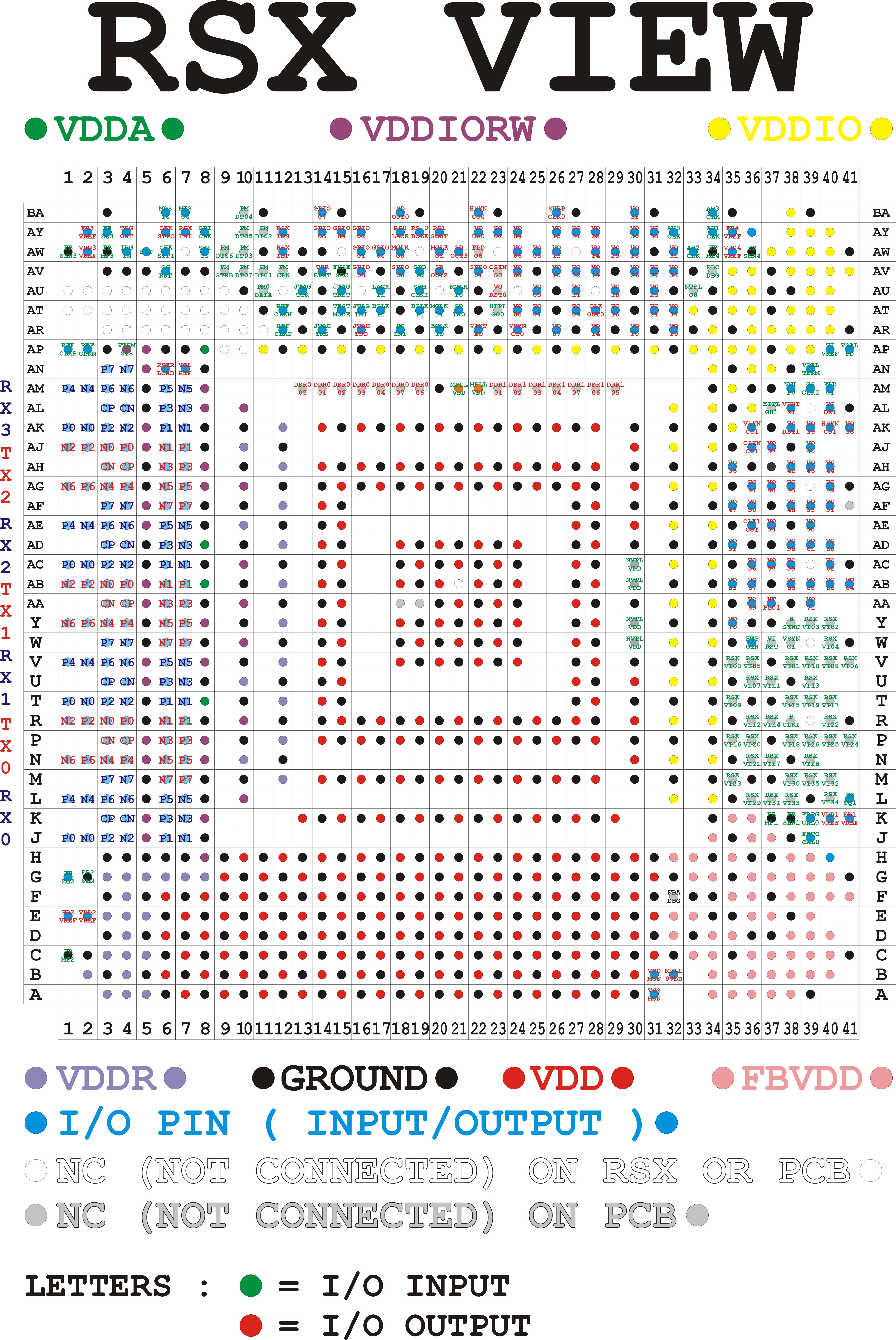
| 38 || P61/SDA0 || || ←I/O→ || Primary I2C bus. UNK_I2C_SDA ? (either HDMI, DVE, or MK) || 0.2v @ standby | | 38 || || P61/SDA0 || || ←I/O→ || Primary I2C bus. UNK_I2C_SDA ? (either HDMI, DVE, or MK) || 0.2v @ standby | ||
|- | |- | ||
! colspan=" | ! colspan="7" | | ||
|- | |- | ||
| 39 || P62 || || ←I/O→ || || 0 | | 39 || || P62 || || ←I/O→ || || 0 | ||
|- | |- | ||
| 40 || {{cellcolors|#c0c0c0}} P63 || P63_DOWN || ←I || 10K resistor to GND || 0 | | 40 || || {{cellcolors|#c0c0c0}} P63 || P63_DOWN || ←I || 10K resistor to GND || 0 | ||
|- | |- | ||
| 41 || {{cellcolors|#ff9933}} <s>P31/TI03/TO03/</s>INTP4 || ACIN_DET || ←I || Connected to pin 4 of the [[Power Supply|PSU]] control connector. See: [[Media:SYSCON_SWx_JTP-001_JSD-001_HSW-001_CN101.jpg|CECH-25xx/SW2/SwitchBoard/PSU schematic]] || 3v @ standby (3.3) | | 41 || || {{cellcolors|#ff9933}} <s>P31/TI03/TO03/</s>INTP4 || ACIN_DET || ←I || Connected to pin 4 of the [[Power Supply|PSU]] control connector. See: [[Media:SYSCON_SWx_JTP-001_JSD-001_HSW-001_CN101.jpg|CECH-25xx/SW2/SwitchBoard/PSU schematic]] || 3v @ standby (3.3) | ||
|- | |- | ||
| 42 || {{cellcolors|#33cc33|#ffffff}} P64/<span style="text-decoration: overline;">RD</span> || || ←I/O→ || Connected (indirectly) to voltage regulator [[Talk:Regulators | BD9684 0906]], pin 4 (enable something) || 0 | | 42 || || {{cellcolors|#33cc33|#ffffff}} P64/<span style="text-decoration: overline;">RD</span> || || ←I/O→ || Connected (indirectly) to voltage regulator [[Talk:Regulators | BD9684 0906]], pin 4 (enable something) || 0 | ||
|- | |- | ||
| 43 || {{cellcolors|#aa7744}} P65/<span style="text-decoration: overline;">WR0</span> || || ←I/O→ || Connected to Pin 12 @ [[Service_Connectors#CN.3F.3F.3F.3F|Service Connector 3rd Gen.]] through a missing SMD component resistor/diode || 3.0 | | 43 || || {{cellcolors|#aa7744}} P65/<span style="text-decoration: overline;">WR0</span> || || ←I/O→ || Connected to Pin 12 @ [[Service_Connectors#CN.3F.3F.3F.3F|Service Connector 3rd Gen.]] through a missing SMD component resistor/diode || 3.0 | ||
|- | |- | ||
| 44 || P66/<span style="text-decoration: overline;">WR1</span> || || ←I/O→ || || 0 | | 44 || || P66/<span style="text-decoration: overline;">WR1</span> || || ←I/O→ || || 0 | ||
|- | |- | ||
| 45 || {{cellcolors|#e0e0e0}} <s>P67/ASTB</s> || NOT_CONNECTED || - || || 0 | | 45 || || {{cellcolors|#e0e0e0}} <s>P67/ASTB</s> || NOT_CONNECTED || - || || 0 | ||
|- | |- | ||
| 46 || P77/EX23/KR7/INTP11 || || ←I/O→ || || 0 | | 46 || || P77/EX23/KR7/INTP11 || || ←I/O→ || || 0 | ||
|- | |- | ||
| 47 || P76/EX22/KR6/INTP10 || || ←I/O→ || || 3v @ standby (3.15) | | 47 || || P76/EX22/KR6/INTP10 || || ←I/O→ || || 3v @ standby (3.15) | ||
|- | |- | ||
| 48 || P75/EX21/KR5/INTP9 || || ←I/O→ || || 3v @ standby (3.15) | | 48 || || P75/EX21/KR5/INTP9 || || ←I/O→ || || 3v @ standby (3.15) | ||
|- | |- | ||
| 49 || {{cellcolors|#c0c0c0}} <s>P74/EX20/KR4/</s>INTP8 || INTP8_DOWN || ←I || 10K resistor to GND || 0 | | 49 || || {{cellcolors|#c0c0c0}} <s>P74/EX20/KR4/</s>INTP8 || INTP8_DOWN || ←I || 10K resistor to GND || 0 | ||
|- | |- | ||
| 50 || {{cellcolors|#aa7744}} P73/EX19/KR3 || || ←I/O→ || Connected to pin 3 @ [[Service_Connectors#CN.3F.3F.3F.3F|Service Connector 3rd Gen.]]. And to voltage regulator [[Talk:Regulators | D35653 0S25]] (FLASH_ENABLE ?) || 0 | | 50 || || {{cellcolors|#aa7744}} P73/EX19/KR3 || || ←I/O→ || Connected to pin 3 @ [[Service_Connectors#CN.3F.3F.3F.3F|Service Connector 3rd Gen.]]. And to voltage regulator [[Talk:Regulators | D35653 0S25]] (FLASH_ENABLE ?) || 0 | ||
|- | |- | ||
| 51 || P72/EX18/KR2 || || ←I/O→ || || 0 | | 51 || || P72/EX18/KR2 || || ←I/O→ || || 0 | ||
|- | |- | ||
| 52 || {{cellcolors|#33cc33|#ffffff}} P71/EX17/KR1 || || ←I/O→ || Connected to voltage regulator [[Talk:Regulators | BD3525]], pin 12 (enable something) || 0 | | 52 || || {{cellcolors|#33cc33|#ffffff}} P71/EX17/KR1 || || ←I/O→ || Connected to voltage regulator [[Talk:Regulators | BD3525]], pin 12 (enable something) || 0 | ||
|- | |- | ||
| 53 || P70/EX16/KR0 || || ←I/O→ || || 0 | | 53 || || P70/EX16/KR0 || || ←I/O→ || || 0 | ||
|- | |- | ||
| 54 || {{cellcolors|#c0c0c0}} P06<s>/<span style="text-decoration: overline;">WAIT</span></s> || P06_DOWN || ←I/O→ || 45K resistor array to GND || 0 | | 54 || || {{cellcolors|#c0c0c0}} P06<s>/<span style="text-decoration: overline;">WAIT</span></s> || P06_DOWN || ←I/O→ || 45K resistor array to GND || 0 | ||
|- | |- | ||
| 55 || {{cellcolors|#c0c0c0}} P05<s>/CLKOUT</s> || P05_DOWN || ←I/O→ || 45K resistor array to GND || 0 | | 55 || || {{cellcolors|#c0c0c0}} P05<s>/CLKOUT</s> || P05_DOWN || ←I/O→ || 45K resistor array to GND || 0 | ||
|- | |- | ||
| 56 || {{cellcolors|#333333|#ffffff}} EV<span style="font-size:60%;">SS1</span> || GND || - || || 0 | | 56 || || {{cellcolors|#333333|#ffffff}} EV<span style="font-size:60%;">SS1</span> || GND || - || || 0 | ||
|- | |- | ||
| 57 || {{cellcolors|#ff3333|#ffffff}} EV<span style="font-size:60%;">DD1</span> || 3.3_EVER_B || - || Connected to standby voltage regulator [[Talk:Regulators|463A]], pin 2 || 3v @ standby (3.3) | | 57 || || {{cellcolors|#ff3333|#ffffff}} EV<span style="font-size:60%;">DD1</span> || 3.3_EVER_B || - || Connected to standby voltage regulator [[Talk:Regulators|463A]], pin 2 || 3v @ standby (3.3) | ||
|- | |- | ||
| 58 || P80/EX0 || || ←I/O→ || || 0 | | 58 || || P80/EX0 || || ←I/O→ || || 0 | ||
|- | |- | ||
| 59 || P81/EX1 || || ←I/O→ || || 0 | | 59 || || P81/EX1 || || ←I/O→ || || 0 | ||
|- | |- | ||
| 60 || P82/EX2 || || ←I/O→ || || 0 | | 60 || || P82/EX2 || || ←I/O→ || || 0 | ||
|- | |- | ||
| 61 || P83/EX3 || || ←I/O→ || || 0 | | 61 || || P83/EX3 || || ←I/O→ || || 0 | ||
|- | |- | ||
| 62 || P84/EX4 || || ←I/O→ || || 0 | | 62 || || P84/EX4 || || ←I/O→ || || 0 | ||
|- | |- | ||
| 63 || P85/EX5 || || ←I/O→ || || 0 | | 63 || || P85/EX5 || || ←I/O→ || || 0 | ||
|- | |- | ||
| 64 || P86/EX6 || || ←I/O→ || || 0 | | 64 || || P86/EX6 || || ←I/O→ || || 0 | ||
|- | |- | ||
! colspan=" | ! colspan="7" | | ||
|- | |- | ||
| 65 || P87/EX7 || || ←I/O→ || || 0 | | 65 || || P87/EX7 || || ←I/O→ || || 0 | ||
|- | |- | ||
| 66 || P30/INTP3/RTC1HZ || || ←I/O→ || || 0 | | 66 || || P30/INTP3/RTC1HZ || || ←I/O→ || || 0 | ||
|- | |- | ||
| 67 || P50/EX8 || || ←I/O→ || || 0 | | 67 || || P50/EX8 || || ←I/O→ || || 0 | ||
|- | |- | ||
| 68 || P51/EX9 || || ←I/O→ || || 0 | | 68 || || P51/EX9 || || ←I/O→ || || 0 | ||
|- | |- | ||
| 69 || P52/EX10 || || ←I/O→ || || 0 | | 69 || || P52/EX10 || || ←I/O→ || || 0 | ||
|- | |- | ||
| 70 || P53/EX11 || || ←I/O→ || || 0 | | 70 || || P53/EX11 || || ←I/O→ || || 0 | ||
|- | |- | ||
| 71 || P54/EX12 || || ←I/O→ || || 0 | | 71 || || P54/EX12 || || ←I/O→ || || 0 | ||
|- | |- | ||
| 72 || P55/EX13 || || ←I/O→ || || 0 | | 72 || || P55/EX13 || || ←I/O→ || || 0 | ||
|- | |- | ||
| 73 || P56/EX14 || || ←I/O→ || || 0 | | 73 || || P56/EX14 || || ←I/O→ || || 0 | ||
|- | |- | ||
| 74 || P57/EX15 || || ←I/O→ || || 0 | | 74 || || P57/EX15 || || ←I/O→ || || 0 | ||
|- | |- | ||
| 75 || {{cellcolors|#33cc33|#ffffff}} P17/EX31/TI02/TO02 || || ←I/O→ || Connected to voltage regulator [[Talk:Regulators | Mitsumi 040 810X]], pin 5 || 0 | | 75 || || {{cellcolors|#33cc33|#ffffff}} P17/EX31/TI02/TO02 || || ←I/O→ || Connected to voltage regulator [[Talk:Regulators | Mitsumi 040 810X]], pin 5 || 0 | ||
|- | |- | ||
| 76 || P16/EX30/TI01/TO01/INTP5 || || ←I/O→ || || 3v @ standby (3.15) | | 76 || || P16/EX30/TI01/TO01/INTP5 || || ←I/O→ || || 3v @ standby (3.15) | ||
|- | |- | ||
| 77 || P15/EX29/RTCDIV/RTCCL || || ←I/O→ || || 3v @ standby (3.3) | | 77 || || P15/EX29/RTCDIV/RTCCL || || ←I/O→ || || 3v @ standby (3.3) | ||
|- | |- | ||
| 78 || {{cellcolors|#aa7744}} <s>P14/EX28/</s>RxD3 || SC_RxD || ←I || SC_RxD UART (terminal).Connected to Pin 11 @ [[Service_Connectors#CN.3F.3F.3F.3F|Service Connector 3rd Gen.]] through a missing SMD component resistor/diode, and to pin 6 @ [[PCI]] Connector || 0 | | 78 || || {{cellcolors|#aa7744}} <s>P14/EX28/</s>RxD3 || SC_RxD || ←I || SC_RxD UART (terminal).Connected to Pin 11 @ [[Service_Connectors#CN.3F.3F.3F.3F|Service Connector 3rd Gen.]] through a missing SMD component resistor/diode, and to pin 6 @ [[PCI]] Connector || 0 | ||
|- | |- | ||
| 79 || {{cellcolors|#aa7744}} <s>P13/EX27/</s>TxD3 || SC_TxD || O→ || SC_TxD UART (terminal).Connected to Pin 10 @ [[Service_Connectors#CN.3F.3F.3F.3F|Service Connector 3rd Gen.]] through a missing SMD component resistor/diode, and to pin 4 @ [[PCI]] Connector || 3.3 | | 79 || || {{cellcolors|#aa7744}} <s>P13/EX27/</s>TxD3 || SC_TxD || O→ || SC_TxD UART (terminal).Connected to Pin 10 @ [[Service_Connectors#CN.3F.3F.3F.3F|Service Connector 3rd Gen.]] through a missing SMD component resistor/diode, and to pin 4 @ [[PCI]] Connector || 3.3 | ||
|- | |- | ||
| 80 || <s>P12/EX26/</s>SO00<s>/TxD0</s> || BE_SPI_DO || O→ || SO from Cell Slave to Syscon Master || 0 | | 80 || || <s>P12/EX26/</s>SO00<s>/TxD0</s> || BE_SPI_DO || O→ || SO from Cell Slave to Syscon Master || 0 | ||
|- | |- | ||
| 81 || <s>P11/EX25/</s>SI00<s>/RxD0</s> || BE_SPI_DI || ←I || SI from Syscon Master to Cell Slave || 1.2 | | 81 || || <s>P11/EX25/</s>SI00<s>/RxD0</s> || BE_SPI_DI || ←I || SI from Syscon Master to Cell Slave || 1.2 | ||
|- | |- | ||
| 82 || <s>P10/EX24/</s><span style="text-decoration: overline;">SCK00</span> || BE_SPI_CLK ? || ←I/O→ || Serial Clock || 0 | | 82 || || <s>P10/EX24/</s><span style="text-decoration: overline;">SCK00</span> || BE_SPI_CLK ? || ←I/O→ || Serial Clock || 0 | ||
|- | |- | ||
| 83 || P90/EX32 || BE_SPI_CS ? || ←I/O→ || Chip Select || 2.0 | | 83 || || P90/EX32 || BE_SPI_CS ? || ←I/O→ || Chip Select || 2.0 | ||
|- | |- | ||
| 84 || P91/EX33 || || ←I/O→ || || 3v @ standby | | 84 || || P91/EX33 || || ←I/O→ || || 3v @ standby | ||
|- | |- | ||
| 85 || P92/EX34 || || ←I/O→ || || 0 | | 85 || || P92/EX34 || || ←I/O→ || || 0 | ||
|- | |- | ||
| 86 || P93/EX35 || || ←I/O→ || || 0 | | 86 || || P93/EX35 || || ←I/O→ || || 0 | ||
|- | |- | ||
| 87 || P94 || || ←I/O→ || RSX_SPI_CS ? See: [[Template:RSX pad layout 41x41]] and [[Media:RSX_SKEMA.jpg|pad AW8@]] || 0 | | 87 || || P94 || || ←I/O→ || RSX_SPI_CS ? See: [[Template:RSX pad layout 41x41]] and [[Media:RSX_SKEMA.jpg|pad AW8@]] || 0 | ||
|- | |- | ||
| 88 || P95/<span style="text-decoration: overline;">SCK11</span>/SCL11 || || ←I/O→ || RSX_SPI_CLK ? See: [[Template:RSX pad layout 41x41]] and [[Media:RSX_SKEMA.jpg|pad AY8@]] || 0 | | 88 || || P95/<span style="text-decoration: overline;">SCK11</span>/SCL11 || || ←I/O→ || RSX_SPI_CLK ? See: [[Template:RSX pad layout 41x41]] and [[Media:RSX_SKEMA.jpg|pad AY8@]] || 0 | ||
|- | |- | ||
| 89 || P96/SI11/SDA11 || || ←I/O→ || RSX_SPI_DI ? See: [[Template:RSX pad layout 41x41]] and [[Media:RSX_SKEMA.jpg|pad BA7@]] || 0 | | 89 || || P96/SI11/SDA11 || || ←I/O→ || RSX_SPI_DI ? See: [[Template:RSX pad layout 41x41]] and [[Media:RSX_SKEMA.jpg|pad BA7@]] || 0 | ||
|- | |- | ||
| 90 || P97/SO11 || || ←I/O→ || RSX_SPI_DO ? See: [[Template:RSX pad layout 41x41]] and [[Media:RSX_SKEMA.jpg|pad BA6@]] || 0 | | 90 || || P97/SO11 || || ←I/O→ || RSX_SPI_DO ? See: [[Template:RSX pad layout 41x41]] and [[Media:RSX_SKEMA.jpg|pad BA6@]] || 0 | ||
|- | |- | ||
| 91 || P112 || || ←I/O→ || || 0 | | 91 || || P112 || || ←I/O→ || || 0 | ||
|- | |- | ||
| 92 || {{cellcolors|#33cc33|#ffffff}} P113 || || ←I/O→ || Connected to voltage regulator [[Talk:Regulators | BD3527 (near FLASH)]], pin 12 || 0 | | 92 || || {{cellcolors|#33cc33|#ffffff}} P113 || || ←I/O→ || Connected to voltage regulator [[Talk:Regulators | BD3527 (near FLASH)]], pin 12 || 0 | ||
|- | |- | ||
| 93 || P114 || || ←I/O→ || || 0 | | 93 || || P114 || || ←I/O→ || || 0 | ||
|- | |- | ||
| 94 || P115 || || ←I/O→ || || 0 | | 94 || || P115 || || ←I/O→ || || 0 | ||
|- | |- | ||
| 95 || {{cellcolors|#33cc33|#ffffff}} P116 || || ←I/O→ || Connected to voltage regulator [[Talk:Regulators | BD3527 (near USB)]], pin 12 || 0 | | 95 || || {{cellcolors|#33cc33|#ffffff}} P116 || || ←I/O→ || Connected to voltage regulator [[Talk:Regulators | BD3527 (near USB)]], pin 12 || 0 | ||
|- | |- | ||
| 96 || P117 || || ←I/O→ || || 0 | | 96 || || P117 || || ←I/O→ || || 0 | ||
|- | |- | ||
| 97 || {{cellcolors|#ff3333|#ffffff}} AV<span style="font-size:60%;">REF1</span> || 3.3_EVER_B || - || Connected to standby voltage regulator [[Talk:Regulators|463A]], pin 2 || 3v @ standby (3.3) | | 97 || || {{cellcolors|#ff3333|#ffffff}} AV<span style="font-size:60%;">REF1</span> || 3.3_EVER_B || - || Connected to standby voltage regulator [[Talk:Regulators|463A]], pin 2 || 3v @ standby (3.3) | ||
|- | |- | ||
| 98 || {{cellcolors|#e0e0e0}} <s>P110/ANO0</s> || NOT_CONNECTED || - || || 0 | | 98 || || {{cellcolors|#e0e0e0}} <s>P110/ANO0</s> || NOT_CONNECTED || - || || 0 | ||
|- | |- | ||
| 99 || {{cellcolors|#e0e0e0}} <s>P111/ANO1</s> || NOT_CONNECTED || - || || 0 | | 99 || || {{cellcolors|#e0e0e0}} <s>P111/ANO1</s> || NOT_CONNECTED || - || || 0 | ||
|- | |- | ||
| 100 || {{cellcolors|#ff3333|#ffffff}} AV<span style="font-size:60%;">REF0</span> || 3.3_EVER_B || - || Connected to standby voltage regulator [[Talk:Regulators|463A]], pin 2 || 3v @ standby (3.3) | | 100 || || {{cellcolors|#ff3333|#ffffff}} AV<span style="font-size:60%;">REF0</span> || 3.3_EVER_B || - || Connected to standby voltage regulator [[Talk:Regulators|463A]], pin 2 || 3v @ standby (3.3) | ||
|- | |- | ||
| 101 || {{cellcolors|#333333|#ffffff}} AV<span style="font-size:60%;">SS0</span> || GND || - || || 0 | | 101 || || {{cellcolors|#333333|#ffffff}} AV<span style="font-size:60%;">SS0</span> || GND || - || || 0 | ||
|- | |- | ||
| 102 || {{cellcolors|#c0c0c0}} <s>P157/</s>ANI15 || ANI15_DOWN || ←I || 100k resistor to GND. And to a missing SMD component to [[Media:Syscon_SW2-303_Unsoldered.JPG|VIA]] to pin 8 of voltage regulator [[Talk:Regulators|463A]] (3.3_EVER_A) <!-- Interesting, the circuit is designed to pull this pin up or down, is down by default but im wondering what does the pullup o0--> || 0 | | 102 || || {{cellcolors|#c0c0c0}} <s>P157/</s>ANI15 || ANI15_DOWN || ←I || 100k resistor to GND. And to a missing SMD component to [[Media:Syscon_SW2-303_Unsoldered.JPG|VIA]] to pin 8 of voltage regulator [[Talk:Regulators|463A]] (3.3_EVER_A) <!-- Interesting, the circuit is designed to pull this pin up or down, is down by default but im wondering what does the pullup o0--> || 0 | ||
|- | |- | ||
! colspan=" | ! colspan="7" | | ||
|- | |- | ||
| 103 || {{cellcolors|#c0c0c0}} <s>P156/</s>ANI14 || ANI14_UP || ←I || [[Media:Syscon_SW2-303_Unsoldered.JPG|VIA]] to 100k resistor to pin 8 of voltage regulator [[Talk:Regulators|463A]] (3.3_EVER_A) || 0 | | 103 || || {{cellcolors|#c0c0c0}} <s>P156/</s>ANI14 || ANI14_UP || ←I || [[Media:Syscon_SW2-303_Unsoldered.JPG|VIA]] to 100k resistor to pin 8 of voltage regulator [[Talk:Regulators|463A]] (3.3_EVER_A) || 0 | ||
|- | |- | ||
| 104 || {{cellcolors|#c0c0c0}} <s>P155/</s>ANI13 || ANI13_DOWN || ←I || [[Media:Syscon_SW2-303_Unsoldered.JPG|VIA]] to 100k resistor to GND || 0 | | 104 || || {{cellcolors|#c0c0c0}} <s>P155/</s>ANI13 || ANI13_DOWN || ←I || [[Media:Syscon_SW2-303_Unsoldered.JPG|VIA]] to 100k resistor to GND || 0 | ||
|- | |- | ||
| 105 || {{cellcolors|#e0e0e0}} <s>P154/ANI12</s> || NOT_CONNECTED || - || || 0 | | 105 || || {{cellcolors|#e0e0e0}} <s>P154/ANI12</s> || NOT_CONNECTED || - || || 0 | ||
|- | |- | ||
| 106 || {{cellcolors|#e0e0e0}} <s>P153/ANI11</s> || NOT_CONNECTED || - || || 0 | | 106 || || {{cellcolors|#e0e0e0}} <s>P153/ANI11</s> || NOT_CONNECTED || - || || 0 | ||
|- | |- | ||
| 107 || {{cellcolors|#e0e0e0}} <s>P152/ANI10</s> || NOT_CONNECTED || - || || 0 | | 107 || || {{cellcolors|#e0e0e0}} <s>P152/ANI10</s> || NOT_CONNECTED || - || || 0 | ||
|- | |- | ||
| 108 || {{cellcolors|#e0e0e0}} <s>P151/ANI9</s> || NOT_CONNECTED || - || || 0 | | 108 || || {{cellcolors|#e0e0e0}} <s>P151/ANI9</s> || NOT_CONNECTED || - || || 0 | ||
|- | |- | ||
| 109 || {{cellcolors|#c0c0c0}} <s>P150/</s>ANI8 || ANI8_UP_UNK || ←I || Connected to an unknown track. And to 10k resistor to [[Media:Syscon_SW2-303_Unsoldered.JPG|VIA]] to pin 8 of voltage regulator [[Talk:Regulators|463A]] (3.3_EVER_A) || 3v @ standby | | 109 || || {{cellcolors|#c0c0c0}} <s>P150/</s>ANI8 || ANI8_UP_UNK || ←I || Connected to an unknown track. And to 10k resistor to [[Media:Syscon_SW2-303_Unsoldered.JPG|VIA]] to pin 8 of voltage regulator [[Talk:Regulators|463A]] (3.3_EVER_A) || 3v @ standby | ||
|- | |- | ||
| 110 || {{cellcolors|#d699ff}} <s>P27/</s>ANI7 || POW_SW_DET || ←I || Power switch detect. Connected to [[switch boards|Switch board]] || 3v @ standby (3.3) 3.3 | | 110 || || {{cellcolors|#d699ff}} <s>P27/</s>ANI7 || POW_SW_DET || ←I || Power switch detect. Connected to [[switch boards|Switch board]] || 3v @ standby (3.3) 3.3 | ||
|- | |- | ||
| 111 || {{cellcolors|#d699ff}} <s>P26/</s>ANI6 || EJECT_SW_DET || ←I || Eject switch detect. Connected to [[switch boards|Switch board]] || 3v @ standby (3.3) 3.3 | | 111 || || {{cellcolors|#d699ff}} <s>P26/</s>ANI6 || EJECT_SW_DET || ←I || Eject switch detect. Connected to [[switch boards|Switch board]] || 3v @ standby (3.3) 3.3 | ||
|- | |- | ||
| 112 || P25/ANI5 || || ←I/O→ || Connected to Wifi/BT module, unknown pad || 0 | | 112 || || P25/ANI5 || || ←I/O→ || Connected to Wifi/BT module, unknown pad || 0 | ||
|- | |- | ||
| 113 || P24/ANI4 || || ←I/O→ || Connected to Wifi/BT module, unknown pad || 0 | | 113 || || P24/ANI4 || || ←I/O→ || Connected to Wifi/BT module, unknown pad || 0 | ||
|- | |- | ||
| 114 || P23/ANI3 || || ←I/O→ || || 0 | | 114 || || P23/ANI3 || || ←I/O→ || || 0 | ||
|- | |- | ||
| 115 || P22/ANI2 || || ←I/O→ || || 0 | | 115 || || P22/ANI2 || || ←I/O→ || || 0 | ||
|- | |- | ||
| 116 || P21/ANI1 || || ←I/O→ || || 0 | | 116 || || P21/ANI1 || || ←I/O→ || || 0 | ||
|- | |- | ||
| 117 || P20/ANI0 || || ←I/O→ || || (0V?) | | 117 || || P20/ANI0 || || ←I/O→ || || (0V?) | ||
|- | |- | ||
| 118 || {{cellcolors|#ff9933}} P130 || ACDC_STBY || O→ || Connected to pin 3 of the [[Power Supply|PSU]] control connector. See: [[Media:SYSCON_SWx_JTP-001_JSD-001_HSW-001_CN101.jpg|CECH-25xx/SW2/SwitchBoard/PSU schematic]] || 3v @ standby (3.3) | | 118 || || {{cellcolors|#ff9933}} P130 || ACDC_STBY || O→ || Connected to pin 3 of the [[Power Supply|PSU]] control connector. See: [[Media:SYSCON_SWx_JTP-001_JSD-001_HSW-001_CN101.jpg|CECH-25xx/SW2/SwitchBoard/PSU schematic]] || 3v @ standby (3.3) | ||
|- | |- | ||
| 119 || {{cellcolors|#33cc33|#ffffff}} P131/TI06/TO06 || || ←I/O→ || Connected to voltage regulator [[Talk:Regulators|348A]], pins 2 and 7 (EN_HDMI & EN_AV together ?... in other words, enable video output) || 3v @ standby (3.3) | | 119 || || {{cellcolors|#33cc33|#ffffff}} P131/TI06/TO06 || || ←I/O→ || Connected to voltage regulator [[Talk:Regulators|348A]], pins 2 and 7 (EN_HDMI & EN_AV together ?... in other words, enable video output) || 3v @ standby (3.3) | ||
|- | |- | ||
| 120 || P07 || || ←I/O→ || || 0 | | 120 || || P07 || || ←I/O→ || || 0 | ||
|- | |- | ||
| 121 || P04/<span style="text-decoration: overline;">SCK10</span>/SCL10 || || ←I/O→ || || 0 | | 121 || || P04/<span style="text-decoration: overline;">SCK10</span>/SCL10 || || ←I/O→ || || 0 | ||
|- | |- | ||
| 122 || P03/SI10/RxD1/SDA10 || || ←I/O→ || || 0 | | 122 || || P03/SI10/RxD1/SDA10 || || ←I/O→ || || 0 | ||
|- | |- | ||
| 123 || P02/SO10/TxD1 || || ←I/O→ || || 0 | | 123 || || P02/SO10/TxD1 || || ←I/O→ || || 0 | ||
|- | |- | ||
| 124 || P01/TO00 || || ←I/O→ || Connected to pin93 @Panasonic [[MN8647091]] || 0 | | 124 || || P01/TO00 || || ←I/O→ || Connected to pin93 @Panasonic [[MN8647091]] || 0 | ||
|- | |- | ||
| 125 || P00/TI00 || || ←I/O→ || || 0 | | 125 || || P00/TI00 || || ←I/O→ || || 0 | ||
|- | |- | ||
| 126 || {{cellcolors|#123456|#ffffff}} <s>P145/TI07/</s>TO07 || FAN_PWM || O→ || PWM Control for the Fan. || 0 | | 126 || || {{cellcolors|#123456|#ffffff}} <s>P145/TI07/</s>TO07 || FAN_PWM || O→ || PWM Control for the Fan. || 0 | ||
|- | |- | ||
| 127 || P144/SO20/TxD2 || || ←I/O→ || (HDMI controller CEC data channel related with pins 1 and 128 ?) || 0 | | 127 || || P144/SO20/TxD2 || || ←I/O→ || (HDMI controller CEC data channel related with pins 1 and 128 ?) || 0 | ||
|- | |- | ||
| 128 || P143/SI20/RxD2/SDA20 || || ←I/O→ || Connected to pin29 @Panasonic [[MN8647091]] (HDMI controller CEC data channel related with pins 1 and 127 ?) || 0 | | 128 || || P143/SI20/RxD2/SDA20 || || ←I/O→ || Connected to pin29 @Panasonic [[MN8647091]] (HDMI controller CEC data channel related with pins 1 and 127 ?) || 0 | ||
|}<includeonly></div></includeonly><noinclude>[[Category:Templates]]</noinclude> | |}<includeonly></div></includeonly><noinclude>[[Category:Templates]]</noinclude> | ||
Revision as of 23:07, 26 June 2021
Pinout


| Pin# | Port | Name | Type | Description | STBY Voltages | |
|---|---|---|---|---|---|---|
| NEC/Renesas | Sony/Custom | |||||
| 1 | P142/SCK20/SCL20 | ←I | Connected to pin27 @Panasonic MN8647091 (HDMI controller CEC data channel related with pins 127 and 128 ?) | 0 | ||
| 2 | SB_INT/SYSCSINT | ←I | Connected to pinD1@SB CXD9963GB through the resistor | ~1V @ standby (0 V?) | ||
| 3 | BE_INT/ATTENTION | ←I | Connected to pinBA17@BE through the NPN transistor (CELL switches the transistor to connect this pin to GND) | 3V @ standby (3.15V) | ||
| 4 | P120/INTP0/EXLVI | ←I/O→ | To +12V_MAIN through the resistor and divider (EXLVI config = External potential input for low-voltage detector ?) | 0 | ||
| 5 | P37 | POW_LED | O→ | Connected to dual led(Green) on Switch board through the dual digital NPN trans. EMH1(SOT-563) | 0 | |
| 6 | P36 | STBY_LED | O→ | Connected to dual led(Red) on Switch board through the dual digital NPN trans. EMH1(SOT-563) | 3v @ standby (3.3V) | |
| 7 | P35 | ←I/O→ | Connected to pinAA18@SB CXD9963GB | 0 | ||
| 8 | P34 | ←I/O→ | Connected to pinAA17@SB CXD9963GB | 0 | ||
| 9 | P33 | ←I/O→ | CELL BE related? | 0 | ||
| 10 | P32 | ←I/O→ | 0 | |||
| 11 | BACK_LEDS | O→ | Connected to Backlit LEDs on Switch board | 0 | ||
| 12 | CONTOUR_LEDS | O→ | Connected to CONTOUR LEDs on Switch board | 0 | ||
| 13 | NOT_CONNECTED | - | Disconnected to GND through a missing SMD component. See: NOWHERE | 0 | ||
| 14 | NOT_CONNECTED | - | Disconnected to GND through a missing SMD component at the other side of the board. See: VIA | 0 | ||
| 15 | P47/INTP2 | ←I/O→ | Unknown purpose. The trace goes in the direction of the Wifi/BT module | 0 | ||
| 16 | BUZZER | O→ | Connected to the base of a transistor that drives a pin of the buzzer to GND | 0 | ||
| 17 | P45/SO01 | ←I/O→ | SB_SPI_DO @CXD9963GB ? | 0 | ||
| 18 | P44/SI01 | ←I/O→ | SB_SPI_DI @CXD9963GB ? | 3v @ standby | ||
| 19 | P43/SCK01 | ←I/O→ | SB_SPI_CLK @CXD9963GB ? | 0 | ||
| 20 | P42/TI04/TO04 | ←I/O→ | SB_SPI_CS @CXD9963GB ? | 0 | ||
| 21 | TOOL_CLK | O→ | Tool clock. Connected to Pin 13 @ Service Connector 3rd Gen. through a missing SMD component resistor/diode | 3.0 | ||
| 22 | TOOL_DAT | ←I/O→ | Tool Data. Connected to Pin 7 @ Service Connector 3rd Gen. through a missing SMD component resistor/diode | 0 | ||
| 23 | P127/SO21 | ←I/O→ | 0 | |||
| 24 | THR_I2C_SDA | ←I/O→ | SMBus data. Connected to pin 7 of CELL/RSX temperature monitors TMP411A/B | 3v @ standby (3.15) | ||
| 25 | THR_I2C_SCL | O→ | SMBus clock. Connected to pin 8 of CELL/RSX temperature monitors TMP411A/B | 3v @ standby (3.15) | ||
| 26 | RESET | RESET | ←I | Connected to Pin 9 @ Service Connector 3rd Gen. through a missing SMD component resistor/diode. And to standby voltage regulator 463A, pin 3 | ||
| 27 | XT_SUB | ←I | Subsystem clock. Connected to a big black crystal. CLK -> 1-2V Amplitude (32.768Khz?) | |||
| 28 | XT_SUB | ←I | Subsystem clock. Connected to a big black crystal. CLK -> 1-2V Amplitude (32.768Khz?) | |||
| 29 | FLMD0 | FLASH_MODE | - | Flash programming mode. Connected to pin 8 @ Service Connector 3rd Gen. through a missing SMD component resistor/diode | 3.33 | |
| 30 | XT_MAIN | ←I | Main system clock. Connected to a tiny metallic crystal marked "EX" | 0.8v @ standby (1.1) | ||
| 31 | XT_MAIN | ←I | Main system clock. Connected to a tiny metallic crystal marked "EX" | 2.2v @ standby (2.4) | ||
| 32 | REGC | VREG_CAP | - | Capacitor for the internal voltage regulator. Connected to ground through a capacitor (around 1uF) at the other side of the board. See: VIA. And 2 diodes to battery+ | ||
| 33 | VSS0 | GND | - | 0 | ||
| 34 | EVSS0 | GND | - | 0 | ||
| 35 | VDD | 3.3_EVER_B | - | Connected to standby voltage regulator 463A, pin 2 | 3v @ standby (3.3) | |
| 36 | EVDD0 | 3.3_EVER_B | - | Connected to standby voltage regulator 463A, pin 2 | 3v @ standby (3.3) | |
| 37 | P60/SCL0 | ←I/O→ | Primary I2C bus. UNK_I2C_SCL ? (either HDMI, DVE, or MK) | 0.2v @ standby | ||
| 38 | P61/SDA0 | ←I/O→ | Primary I2C bus. UNK_I2C_SDA ? (either HDMI, DVE, or MK) | 0.2v @ standby | ||
| 39 | P62 | ←I/O→ | 0 | |||
| 40 | P63 | P63_DOWN | ←I | 10K resistor to GND | 0 | |
| 41 | ACIN_DET | ←I | Connected to pin 4 of the PSU control connector. See: CECH-25xx/SW2/SwitchBoard/PSU schematic | 3v @ standby (3.3) | ||
| 42 | P64/RD | ←I/O→ | Connected (indirectly) to voltage regulator BD9684 0906, pin 4 (enable something) | 0 | ||
| 43 | P65/WR0 | ←I/O→ | Connected to Pin 12 @ Service Connector 3rd Gen. through a missing SMD component resistor/diode | 3.0 | ||
| 44 | P66/WR1 | ←I/O→ | 0 | |||
| 45 | NOT_CONNECTED | - | 0 | |||
| 46 | P77/EX23/KR7/INTP11 | ←I/O→ | 0 | |||
| 47 | P76/EX22/KR6/INTP10 | ←I/O→ | 3v @ standby (3.15) | |||
| 48 | P75/EX21/KR5/INTP9 | ←I/O→ | 3v @ standby (3.15) | |||
| 49 | INTP8_DOWN | ←I | 10K resistor to GND | 0 | ||
| 50 | P73/EX19/KR3 | ←I/O→ | Connected to pin 3 @ Service Connector 3rd Gen.. And to voltage regulator D35653 0S25 (FLASH_ENABLE ?) | 0 | ||
| 51 | P72/EX18/KR2 | ←I/O→ | 0 | |||
| 52 | P71/EX17/KR1 | ←I/O→ | Connected to voltage regulator BD3525, pin 12 (enable something) | 0 | ||
| 53 | P70/EX16/KR0 | ←I/O→ | 0 | |||
| 54 | P06 |
P06_DOWN | ←I/O→ | 45K resistor array to GND | 0 | |
| 55 | P05 |
P05_DOWN | ←I/O→ | 45K resistor array to GND | 0 | |
| 56 | EVSS1 | GND | - | 0 | ||
| 57 | EVDD1 | 3.3_EVER_B | - | Connected to standby voltage regulator 463A, pin 2 | 3v @ standby (3.3) | |
| 58 | P80/EX0 | ←I/O→ | 0 | |||
| 59 | P81/EX1 | ←I/O→ | 0 | |||
| 60 | P82/EX2 | ←I/O→ | 0 | |||
| 61 | P83/EX3 | ←I/O→ | 0 | |||
| 62 | P84/EX4 | ←I/O→ | 0 | |||
| 63 | P85/EX5 | ←I/O→ | 0 | |||
| 64 | P86/EX6 | ←I/O→ | 0 | |||
| 65 | P87/EX7 | ←I/O→ | 0 | |||
| 66 | P30/INTP3/RTC1HZ | ←I/O→ | 0 | |||
| 67 | P50/EX8 | ←I/O→ | 0 | |||
| 68 | P51/EX9 | ←I/O→ | 0 | |||
| 69 | P52/EX10 | ←I/O→ | 0 | |||
| 70 | P53/EX11 | ←I/O→ | 0 | |||
| 71 | P54/EX12 | ←I/O→ | 0 | |||
| 72 | P55/EX13 | ←I/O→ | 0 | |||
| 73 | P56/EX14 | ←I/O→ | 0 | |||
| 74 | P57/EX15 | ←I/O→ | 0 | |||
| 75 | P17/EX31/TI02/TO02 | ←I/O→ | Connected to voltage regulator Mitsumi 040 810X, pin 5 | 0 | ||
| 76 | P16/EX30/TI01/TO01/INTP5 | ←I/O→ | 3v @ standby (3.15) | |||
| 77 | P15/EX29/RTCDIV/RTCCL | ←I/O→ | 3v @ standby (3.3) | |||
| 78 | SC_RxD | ←I | SC_RxD UART (terminal).Connected to Pin 11 @ Service Connector 3rd Gen. through a missing SMD component resistor/diode, and to pin 6 @ PCI Connector | 0 | ||
| 79 | SC_TxD | O→ | SC_TxD UART (terminal).Connected to Pin 10 @ Service Connector 3rd Gen. through a missing SMD component resistor/diode, and to pin 4 @ PCI Connector | 3.3 | ||
| 80 | BE_SPI_DO | O→ | SO from Cell Slave to Syscon Master | 0 | ||
| 81 | BE_SPI_DI | ←I | SI from Syscon Master to Cell Slave | 1.2 | ||
| 82 | BE_SPI_CLK ? | ←I/O→ | Serial Clock | 0 | ||
| 83 | P90/EX32 | BE_SPI_CS ? | ←I/O→ | Chip Select | 2.0 | |
| 84 | P91/EX33 | ←I/O→ | 3v @ standby | |||
| 85 | P92/EX34 | ←I/O→ | 0 | |||
| 86 | P93/EX35 | ←I/O→ | 0 | |||
| 87 | P94 | ←I/O→ | RSX_SPI_CS ? See: Template:RSX pad layout 41x41 and pad AW8@ | 0 | ||
| 88 | P95/SCK11/SCL11 | ←I/O→ | RSX_SPI_CLK ? See: Template:RSX pad layout 41x41 and pad AY8@ | 0 | ||
| 89 | P96/SI11/SDA11 | ←I/O→ | RSX_SPI_DI ? See: Template:RSX pad layout 41x41 and pad BA7@ | 0 | ||
| 90 | P97/SO11 | ←I/O→ | RSX_SPI_DO ? See: Template:RSX pad layout 41x41 and pad BA6@ | 0 | ||
| 91 | P112 | ←I/O→ | 0 | |||
| 92 | P113 | ←I/O→ | Connected to voltage regulator BD3527 (near FLASH), pin 12 | 0 | ||
| 93 | P114 | ←I/O→ | 0 | |||
| 94 | P115 | ←I/O→ | 0 | |||
| 95 | P116 | ←I/O→ | Connected to voltage regulator BD3527 (near USB), pin 12 | 0 | ||
| 96 | P117 | ←I/O→ | 0 | |||
| 97 | AVREF1 | 3.3_EVER_B | - | Connected to standby voltage regulator 463A, pin 2 | 3v @ standby (3.3) | |
| 98 | NOT_CONNECTED | - | 0 | |||
| 99 | NOT_CONNECTED | - | 0 | |||
| 100 | AVREF0 | 3.3_EVER_B | - | Connected to standby voltage regulator 463A, pin 2 | 3v @ standby (3.3) | |
| 101 | AVSS0 | GND | - | 0 | ||
| 102 | ANI15_DOWN | ←I | 100k resistor to GND. And to a missing SMD component to VIA to pin 8 of voltage regulator 463A (3.3_EVER_A) | 0 | ||
| 103 | ANI14_UP | ←I | VIA to 100k resistor to pin 8 of voltage regulator 463A (3.3_EVER_A) | 0 | ||
| 104 | ANI13_DOWN | ←I | VIA to 100k resistor to GND | 0 | ||
| 105 | NOT_CONNECTED | - | 0 | |||
| 106 | NOT_CONNECTED | - | 0 | |||
| 107 | NOT_CONNECTED | - | 0 | |||
| 108 | NOT_CONNECTED | - | 0 | |||
| 109 | ANI8_UP_UNK | ←I | Connected to an unknown track. And to 10k resistor to VIA to pin 8 of voltage regulator 463A (3.3_EVER_A) | 3v @ standby | ||
| 110 | POW_SW_DET | ←I | Power switch detect. Connected to Switch board | 3v @ standby (3.3) 3.3 | ||
| 111 | EJECT_SW_DET | ←I | Eject switch detect. Connected to Switch board | 3v @ standby (3.3) 3.3 | ||
| 112 | P25/ANI5 | ←I/O→ | Connected to Wifi/BT module, unknown pad | 0 | ||
| 113 | P24/ANI4 | ←I/O→ | Connected to Wifi/BT module, unknown pad | 0 | ||
| 114 | P23/ANI3 | ←I/O→ | 0 | |||
| 115 | P22/ANI2 | ←I/O→ | 0 | |||
| 116 | P21/ANI1 | ←I/O→ | 0 | |||
| 117 | P20/ANI0 | ←I/O→ | (0V?) | |||
| 118 | P130 | ACDC_STBY | O→ | Connected to pin 3 of the PSU control connector. See: CECH-25xx/SW2/SwitchBoard/PSU schematic | 3v @ standby (3.3) | |
| 119 | P131/TI06/TO06 | ←I/O→ | Connected to voltage regulator 348A, pins 2 and 7 (EN_HDMI & EN_AV together ?... in other words, enable video output) | 3v @ standby (3.3) | ||
| 120 | P07 | ←I/O→ | 0 | |||
| 121 | P04/SCK10/SCL10 | ←I/O→ | 0 | |||
| 122 | P03/SI10/RxD1/SDA10 | ←I/O→ | 0 | |||
| 123 | P02/SO10/TxD1 | ←I/O→ | 0 | |||
| 124 | P01/TO00 | ←I/O→ | Connected to pin93 @Panasonic MN8647091 | 0 | ||
| 125 | P00/TI00 | ←I/O→ | 0 | |||
| 126 | FAN_PWM | O→ | PWM Control for the Fan. | 0 | ||
| 127 | P144/SO20/TxD2 | ←I/O→ | (HDMI controller CEC data channel related with pins 1 and 128 ?) | 0 | ||
| 128 | P143/SI20/RxD2/SDA20 | ←I/O→ | Connected to pin29 @Panasonic MN8647091 (HDMI controller CEC data channel related with pins 1 and 127 ?) | 0 | ||