Card Adapter
PlayStation Card Adapter
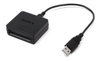
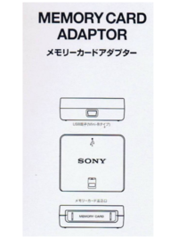
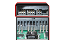
The PlayStation 3 Memory Card Adaptor is a peripheral device that allows data to be transferred from a PlayStation or PlayStation 2 memory card to the PlayStation 3's hard disk.
Technical Specifications
| Overview of Technical Specifications | |
|---|---|
| Product Code | CECHZM1 (SCPH-98042) |
| External Dimension | approximately 58mm x 50mm x 20mm (height x width x depth) |
| Weight | approximately 50g |
| Cable Length | USB Cord length / USB hub |
| Connection Type | USB |
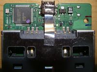
| Program Memory | 64KB (64K x 8) - Flash (2211UFP24V H8S/2211 seen on CECHZM1 j) |
| PS3 FW related | 1.80 |
| Mountpoint | dev_MCA ( from Memory card utility PS/PS2). |
Functions
- On lower FW, You could not copy saves back to a physical Memory Card. You can copy them between PS3 internal virtual memory cards, but not back to a physical PSone or PS2 card (but possible on 3.55).
- On lower FW, You could not explore your PSone or PS2 card and copy over specific game saves, but you can delete saves, once the card has been copied over to the hard drive (but possible on 3.55).
- The adaptor will not work with cards that have more than 8MB of storage space.
- PocketStation can be use (and recognized as) with the PS3 card adapter.
- USB hub works.
Analysis
USB
Device Descriptor
| Device Descriptor | ||||
|---|---|---|---|---|
| Offset | Field | Size | Value | Description |
| 0 | bLength | 1 | 0x12 | Size of this descriptor in bytes (18) |
| 1 | bDescriptorType | 1 | 0x01 | DEVICE descriptor type (Constant = 1) |
| 2 | bcdUSB | 2 | 0x0110 | USB Spec release number (1.10):
with which the device and is descriptors are compliant (e.g.: 0x0200 (USB2.0), 0x0300, (USB_3.0|USB3.0)) |
| 4 | bDeviceClass | 1 | 0xFF | Class code assigned by USB-IF:
(used by the operating system to find a class driver for your device)
|
| 5 | bDeviceSubClass | 1 | 0x00 | SubClass Code assigned by USB-IF
(used by the operating system to find a class driver for your device) |
| 6 | bDeviceProtocol | 1 | 0xFF | Protocol Code assigned by USB-IF
(used by the operating system to find a class driver for your device) |
| 7 | bMaxPacketSize0 | 1 | 0x40 | Max packet size for endpoint 0. (64)
|
| 8 | idVendor | 2 | 0x054C | Vendor ID (VID) (Sony Corp.)
must be obtained from USB-IF (used by the operating system to find a driver for your device) |
| 10 | idProduct | 2 | 0x02ea | Product ID (PID) - (PlayStation 3 Memory Card Adaptor)
assigned by the manufacturer (used by the operating system to find a driver for your device) |
| 12 | bcdDevice | 2 | 0x0100 | Device release number (Version: 1.00)
in binary coded decimal |
| 14 | iManufacturer | 1 | 0x00 | Index of string descriptor describing manufacturer
set to 0 if no string |
| 15 | iProduct | 1 | 0x00 | Index of string descriptor describing product
set to 0 if no string |
| 16 | iSerialNumber | 1 | 0x00 | Index of string descriptor describing device serial number set to 0 if no string |
| 17 | bNumConfigurations | 1 | 0x01 | Number of possible configurations |
Configuration Descriptor
| Configuration Descriptor | |||||||||||
|---|---|---|---|---|---|---|---|---|---|---|---|
| Offset | Field | Size | Value | Description | |||||||
| 0 | bLength | 1 | 0x09 | Size | |||||||
| 1 | bDescriptorType | 1 | 0x02 | (= 2) | |||||||
| 2 | wTotalLength | 2 | 0x0027 | Total number of bytes (39) in this descriptor and all the following descriptors (9+9+7+7+7) | |||||||
| 4 | bNumInterfaces | 1 | 0x01 | Number of interfaces supported by this configuration | |||||||
| 5 | bConfigurationValue | 1 | 0x01 | Value used by Set Configuration to select this configuration | |||||||
| 6 | iConfiguration | 1 | 0x00 | Index of string descriptor describing configuration - set to 0 if no string | |||||||
| 7 | bmAttributes | 1 | 0x80 | Powered by the bus (10000000)
specify power parameters for the configuration :
| |||||||
| 8 | bMaxPower | 1 | 0x64 | Maximum current: 200mA drawn by device in this configuration. In units of 2mA. So 0x32 (50) means 100 mA | |||||||
Interface Descriptor
| Interface Descriptor | ||||
|---|---|---|---|---|
| 0 | bLength | 1 | 0x09 | Size |
| 1 | bDescriptorType | 1 | 0x04 | (= 4) |
| 2 | bInterfaceNumber | 1 | 0x00 | Number identifying this interface.
Zero-based value |
| 3 | bAlternateSetting | 1 | 0x00 | The first (and default) value used to select alternative setting is always 0
(An interface can have more than one variant, and these variants can be switched between, while other interfaces are still in operation) |
| 4 | bNumEndpoints | 1 | 0x03 | Number of Endpoints used for this interface |
| 5 | bInterfaceClass | 1 | 0xFF | Class code assigned by USB-IF]
|
| 6 | bInterfaceSubClass | 1 | 0x00 | SubClass Code assigned by USB-IF |
| 7 | bInterfaceProtocol | 1 | 0xFF | Protocol Code assigned by USB-IF |
| 8 | iInterface | 1 | 0x00 | Index of string descriptor describing interface - set to 0 if no string |
Endpoint Descriptor
| Endpoint (IN) Descriptor | ||||
|---|---|---|---|---|
| 0 | bLength | 1 | 0x07 | Size |
| 1 | bDescriptorType | 1 | 0x05 | (= 5) |
| 2 | bEndpointAddress | 1 | 0x81 | IN <--(10 00 0001)--> 1
The address of this endpoint within the device:
|
| 3 | bmAttributes | 1 | 0x02 | Interrupt (00000010)
(D1:0) Transfer Type:
The following only apply to isochronous endpoints. Else set to 0. (D3:2) Synchronisation Type (ISO mode):
(D5:4) Usage Type (ISO mode):
(D7:6) Reserved Set to 0 |
| 4 | wMaxPacketSize | 2 | 0x0040 | (64) |
| 6 | bInterval | 1 | 0x00 | (unit depends on device speed)
Interval for polling endpoint for data transfers. Expressed in frames (ms) for low/full speed or microframes (125μs) for high speed |
| Endpoint (OUT) Descriptor | ||||
| 0 | bLength | 1 | 0x07 | Size |
| 1 | bDescriptorType | 1 | 0x05 | (= 5) |
| 2 | bEndpointAddress | 1 | 0x02 | OUT<-- (00 00 0010)-->2 |
| 3 | bmAttributes | 1 | 0x02 | Bulk |
| 4 | wMaxPacketSize | 2 | 0x0040 | (64) |
| 6 | bInterval | 1 | 0x00 | |
| Endpoint (IN) Descriptor | ||||
| 0 | bLength | 1 | 0x07 | Size |
| 1 | bDescriptorType | 1 | 0x05 | (= 5) |
| 2 | bEndpointAddress | 1 | 0x83 | IN<-- (10 00 0011)-->3 |
| 3 | bmAttributes | 1 | 0x03 | Interrupt |
| 4 | wMaxPacketSize | 2 | 0x0001 | (1 byte) |
| 6 | bInterval | 1 | 0x64 | 100 |
Free MC boot install with PS3 Memory Card Adapter (CECHZM1)
http://www.ps3devwiki.com/files/Homebrew/ps3mca/
- You can now install FMCB from a PC to MC with these MC-Adapters!
- You can sign MC-KELFs to your MCs directly from PC!
- You can make multi-region-installs!
- The FMCB1.8c-Loader finally includes the V0-Kernel-Fix for those old SCPH-1x000-Consoles (this gives users of those old models the ability to run a few homebrew-apps, which were previously incompatible to those versions)!
We recently found a new way to install FMCB with the PlayStation3 Memory Card Adaptor (CECHZM1) connected to your PC. Since this device is somewhat cheap, it could be a good alternate way for those who don't have access to an already hacked PS2. The method consist of a command line software and using set of commands (or scripts) in order to install the FMBC hack properly. It also has the advantage to do a multi region/models installation. One restriction is that the software doesn't work with Datel's MC (mainly related with setting a proper termination code for communications) and maybe with some other brands, however it was tested successfully with official 8MB Memory Cards and with some crappy Chinese clones too. Currently the FMCB loader being installed is v1.8c which contain an important kernel fix for the 10K. The util to allow to communicate and sign the file for the MC was made by me and "someone who wants to stay anonymous". Note that without this anonymous contributor it would have been impossible to achieve it. git repository: https://github.com/jimmikaelkael/ps3mca-tool
- http://www.mirrorcreator.com/files/10IHXLCZ/ps3mca-windrv.zip_links (driver)
- http://www.mirrorcreator.com/files/0TTXY1K0/ps3mca-tool-fmcb-1.8c.zip_links (precompiled Windows/Linux)
- http://www.mirrorcreator.com/files/XVFKCQ6R/jimmikaelkael-ps3mca-tool-12a198f.zip_links (source) mirror mirror
Memory Card
The Playstation Memory Cards have an interface similar to the Controller Port, which is similar to SPI. They normally have 1 Mb or 128 Kilobyte of EEprom memory. Serial data transfer is LSB-First format. Some bigger non-Sony Cards use internal bankswitching (Multiple virtual Cards with a button switching to the next bank each press / alternatively some do not have a button but rely on buttoncombos with the Dualshock controller). Other bigger non-Sony Cards (e.g. Datel MAX 16MB, 32MB, 64MB, 128MB, 256MB) address it as a single card (and thus can be rely slow).
Sony Playstation Memory Card (SCPH-1020)
Aside from the Sanyo LC86F8604A chip, the board additionally contains some resistors, capacitors, z-diodes (for protection against too high voltages), a 6MHz oscillator (for the CPU), and a 5pin reset generator (on the cart edge connector, the supply pins are slightly longer than the data signal pins, so when inserting the cartridge, power/reset gets triggered first; the 7.5V supply pin is left unconnected, only 3.5V are used).
SONY CXD8732AQ
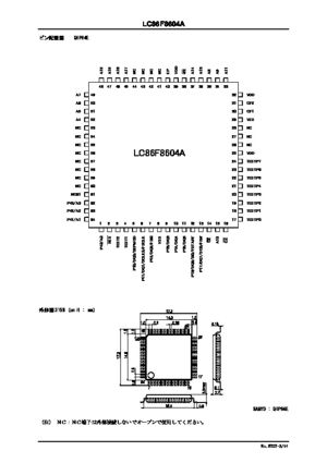
The "SONY CXD8732AQ" chip is installed on memory cards with "SPC02K1020B" boards, however, the text layer on the board says that it's an "LC86F8604A" chip. So, the CXD8732AQ is most probably a standard LC86F8604A chip with a Sony Memory Card BIOS ROM on it. The "SONY CXD8732AQ" comes in a huge 64 QFP pin package, but it connects only to:
 5 = /IRQ7   (via 22 ohm)         2 = /RESET (from U2)
 6 = JOYCLK  (via 220 ohm)        30,31 = CF1,CF2 (12 clock pulses per 2us)
 7 = /JOYn   (via 220 ohm)        14,16,25,32,38,39,61 = 3.5V (via 3.3 ohm)
 12 = JOYCMD (via 220 ohm)        8,15,28,29 = GND
 13 = JOYDAT (via 22 ohm)         All other pins = Not connected
Caution: The "diagonal edge" at the upper-left of the CXD8732AQ chip is Pin 49 (not pin 1), following the pin numbers on the board (and the Sanyo datasheet pinouts), pin 1 is at the lower-left (near the dot mark) and follow a counterclockwise move notation.
- standard Sanyo LC86F8604A chip datasheet :
- www.digchip.com/datasheets/parts/datasheet/413/LC86F8604A.php
Features
- Flash memory erase and rewrite at a power-supply voltage of 2.8 V achieved for the first time in the industry.
- 132-KB on-chip flash memory
- 2.8-V single-voltage power supply
- On-board reprogramming function
- The flash memory can be erased in 128-byte block units.
Specifications
- Sanyo original 8-bit CPU core (Minimum bus cycle time: 0.5 µs, minimum instruction cycle time: 1 µs)
- 132 KB of flash memory and 256 bytes of RAM on chip
- Two 8-bit timers
- 8-bit synchronous serial interface
Pinout
The controller port is exactly the same electricly as the memory card port (with an extra pin, which could be used as lightpen input but most or all controllers leave the pin unused.
   1  2   3  4  5   6  7  8
 ----------------------------
 | o  o | o  o  o | o  o  o |  (at the Card)
 \__________________________/
| Pin № | Name | I/O | Description |
|---|---|---|---|
| 1 | DATA | O | Data from card (MISO) - JOYDAT |
| 2 | CMD | I | Command/Data to card (MOSI) - JOYCMD |
| 3 | VCChigh | N.C. | +7.6 VDC power source for Joypad/rumble (never used for flashmemory) |
| 4 | Ground | GND | Ground |
| 5 | VCClow | I | Vcc (+3.6 VDC) |
| 6 | /ATT | I | Select (SS) pad or memory-card - /JOY1,/JOY2 Selects controller/memorycard 1 (left), or controller/memorycard 2 (right) |
| 7 | CLK | I | Clock (SCK) - JOYCLK |
| 8 | /ACK | O | Acknowledge /IRQ7 |
Notes:
- A maximum of two 4-way splitters can be used, one on each main port, for a maximum of 8 controllers and 8 memorycards (Signal Select [SS] for PAD1, PAD2 is separated)
- Direction is relative to card. I = Input, O = Output, N.C = Not Connected.
Signals
DATA
Signal from Card to PS1/PSone. This signal is an 8 bit serial transmission synchronous to the falling edge of clock (Both the incoming and outgoing signals change on a high to low transition of clock. All the reading of signals is done on the leading edge to allow settling time).
COMMAND
Signal from PS1/PSone to Card. This signal is the counter part of DATA. It is again an 8 bit serial transmission on the falling edge of clock.
VCC
VCC 3.6VDC. The main board in the PS1/PSone has 2 surface mount 750mA fuses, one for each port
ATT
ATT is used to get the attention of the card. This signal will go low for the duration of a transmission. Time is 16msec between SEL from previous SEL.
CLOCK
Signal (high) from PS1/PSone to card. Used to keep units in sync. 250kHz clock for PlayStation.
ACK
Acknowledge signal from Card to PS1/PSone. This signal should go low for at least one clock period after each 8 bits are sent and ATT is still held low. If the ACK signal does not go low within about 60μsec the PS1/PSone will then start interrogating other devices.
Sources
- http://www.hardwarebook.info/Sony_Playstation_Memory_Card
- http://www.raphnet.net/electronique/psx_adaptor/Playstation.txt
Misc
This simple mod (adding Led) also works with PS1 Memory Card plugged into the Memory Card Adaptor or the Memory Card Adaptor itself:
- http://www.youtube.com/watch?v=be5rSKFuxJY //video should be removed because it s a mess, but before need more infos/photos/wiki format
Video s comment:
you need 32 guage insulated wire and 3mm LED (does not matter what color...) and you drill the hole
(without the chip inside to avoid damage) 2 - 3mm  from the left side on the outward edge.
Official PS2 Memory Card pins are numbered (8: negative & 5: positive), official PS1 Memory Card hole for the led can be more centred.
Sony Documentation
- manuals.playstation.net
| |||||||||||||
