GL3520
Jump to navigation
Jump to search
Genesys Logic GL3520

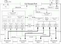
Genesys Logic GL3520 Block Diagram
USB 3.0 MTT Hub Controller
Product page : http://www.genesyslogic.com/en/product_view.php?show=26
Datasheet :
- http://www.arrivalelectronics.co.uk/uploads/GL3520-21+Datasheet_101.pdf
- http://u.jimdo.com/www102/o/sa2984366ace24167/download/m223efb67d8a85ed6/1322800153/GL3520+Datasheet_132.pdf
GL3520 Firmware ISP Tool + User Guide :
- ...
Pinout


| Pin | Name | Type | Description |
|---|---|---|---|
| 1 | PAMBER4 | B (pd) | Amber LED indicator for DSPORT4 |
| 2 | PWREN4J | B | Active low. Power enable output for DSPORT4 |
| 3 | RTERM | A | A 680ohm resister must be connected between RTERM and Ground |
| 4 | NC | - | No Connection |
| 5 | NC | - | No Connection |
| 6 | X1 | I | 25MHz Crystal / OSC clock input |
| 7 | X2 | O | 25MHz Crystal / OSC clock output. |
| 8 | NC | - | No Connection |
| 9 | TXN_UP | O | USB 3.0 Differential Data Transmitter TX- of USPORT |
| 10 | TXP_UP | O | USB 3.0 Differential Data Transmitter TX+ of USPORT |
| 11 | GND | P | Digital/Analog ground |
| 12 | RXN_UP | I | USB 3.0 Differential Data Receiver RX-+ of USPORT |
| 13 | RXP_UP | I | USB 3.0 Differential Data Receiver RX+ of USPORT |
| 14 | VP12 | P | Analog 1.2V power input for Analog circuit |
| 15 | VP12 | P | Analog 1.2V power input for Analog circuit |
| 16 | TXN_DS1 | O | USB 3.0 Differential Data Transmitter TX- of DSPORT1 |
| 17 | TXP_DS1 | O | USB 3.0 Differential Data Transmitter TX-/TX+ of DSPORT1 |
| 18 | GND | P | Digital/Analog ground |
| 19 | RXN_DS1 | I | USB 3.0 Differential Data Receiver RX- of DSPORT1 |
| 20 | RXP_DS1 | I | USB 3.0 Differential Data Receiver RX+ of DSPORT1 |
| 21 | VP12 | P | Analog 1.2V power input for Analog circuit |
| 22 | NC | - | No Connection |
| 23 | VP12 | P | Analog 1.2V power input for Analog circuit |
| 24 | TXN_DS2 | O | USB 3.0 Differential Data Transmitter TX- of DSPORT2 |
| 25 | TXP_DS2 | O | USB 3.0 Differential Data Transmitter TX+ of DSPORT2 |
| 26 | GND | P | Digital/Analog ground |
| 27 | RXN_DS2 | I | USB 3.0 Differential Data Receiver RX- of DSPORT2 |
| 28 | RXP_DS2 | I | USB 3.0 Differential Data Receiver RX+ of DSPORT2 |
| 29 | VP12 | P | Analog 1.2V power input for Analog circuit |
| 30 | VP12 | P | Analog 1.2V power input for Analog circuit |
| 31 | TXN_DS3 | O | USB 3.0 Differential Data Transmitter TX- of DSPORT3 |
| 32 | TXP_DS3 | O | USB 3.0 Differential Data Transmitter TX+ of DSPORT3 |
| 33 | GND | P | Digital/Analog ground |
| 34 | RXN_DS3 | I | USB 3.0 Differential Data Receiver RX- of DSPORT3 |
| 35 | RXP_DS3 | I | USB 3.0 Differential Data Receiver RX+ of DSPORT3 |
| 36 | VP12 | P | Analog 1.2V power input for Analog circuit |
| 37 | VP12 | P | Analog 1.2V power input for Analog circuit |
| 38 | TXN_DS4 | O | USB 3.0 Differential Data Transmitter TX- of DSPORT4 |
| 39 | TXP_DS4 | O | USB 3.0 Differential Data Transmitter TX+ of DSPORT4 |
| 40 | GND | P | Digital/Analog ground |
| 41 | RXN_DS4 | I | USB 3.0 Differential Data Receiver RX- of DSPORT4 |
| 42 | RXP_DS4 | I | USB 3.0 Differential Data Receiver RX+ of DSPORT4 |
| 43 | VP12 | P | Analog 1.2V power input for Analog circuit |
| 44 | DVDD12 | P | 1.2V digital power input for digital circuits |
| 45 | OVCUR2J | I (pu) | Active low. Over current indicator for DSPORT2 |
| 46 | PWREN2J | B | Active low. Power enable output for DSPORT2 |
| 47 | PWREN3J | B | Active low. Power enable output for DSPORT3 |
| 48 | PGREEN3 | B (pd) | Green LED indicator for DSPORT3 |
| 49 | DVDD12 | P | 1.2V digital power input for digital circuits |
| 50 | P_SPI_CK | B | For SPI data clock |
| 51 | P_SPI_CZ | B | For SPI data chip enable |
| 52 | PAMBER1 | B (pd) | Amber LED indicator for DSPORT1 |
| 53 | PWREN1J | B | Active low. Power enable output for DSPORT1 PWREN1# is the only power-enable output for GANG mode |
| 54 | OVCUR4J | I (pu) | Active low. Over current indicator for DSPORT1 |
| 55 | VBUS | I | VBUS valid input |
| 56 | PAMBER3 | B (pd) | Amber LED indicator for DSPORT3 |
| 57 | DVDD12 | P | 1.2V digital power input for digital circuits |
| 58 | DVDD | P | 3.3V digital power input for digital circuits |
| 59 | DM0 | B | USB 2.0 DM for USPORT |
| 60 | DP0 | B | USB 2.0 DP for USPORT |
| 61 | DM1 | B | USB 2.0 DM for DSPORT1 |
| 62 | DP1 | B | USB 2.0 DP for DSPORT1 |
| 63 | AVDD | P | Analog 3.3V power input |
| 64 | DM2 | B | USB 2.0 DM for DSPORT2 |
| 65 | DP2 | B | USB 2.0 DP for DSPORT2 |
| 66 | AVDD1 | P | Analog 3.3V power input |
| 67 | GND | P | Digital/Analog ground |
| 68 | DM3 | B | USB 2.0 DM for DSPORT3 |
| 69 | DP3 | B | USB 2.0 DP for DSPORT3 |
| 70 | AVDD | P | Analog 3.3V power input |
| 71 | DM4 | B | USB 2.0 DM for DSPORT4 |
| 72 | DP4 | B | USB 2.0 DP for DSPORT4 |
| 73 | DVDD | P | 3.3V digital power input for digital circuits |
| 74 | PGANG | I | Default put in input mode after power-on reset. Individual/gang mode is strapped during this period. |
| 75 | DVDD12 | P | 1.2V digital power input for digital circuits |
| 76 | TEST | B (pd) | TEST: 0: Normal operation. 1: Chip will be put in test mode. |
| 77 | OVCUR3J | I (pu) | Active low. Over current indicator for DSPORT3 |
| 78 | OVCUR1J | I (pu) | Active low. Over current indicator for DSPORT1 OVCUR1# is the only over current flag for GANG mode |
| 79 | PGREEN1 | B (pd) | Green LED indicator for DSPORT1 |
| 80 | P_SPI_DO | B | For SPI data Input |
| 81 | P_SPI_DI | B | For SPI data Output |
| 82 | PSELF | I | 0: GL3520 is bus-powered. 1: GL3520 is self-powered. |
| 83 | RESETJ | I (pd) | Active low. External reset input, default pull high 10KΩ. When RESET# = low, whole chip is reset to the initial state |
| 84 | PGREEN2 | B (pd) | Green LED indicator for DSPORT2 |
| 85 | V33 | P | 5V-to-3.3V regulator Vout & 3.3 input |
| 86 | V5 | P | 5V Power input. It need be NC if using external regulator |
| 87 | PAMBER2 | B (pd) | Amber LED indicator for DSPORT2 |
| 88 | PGREEN4 | B (pd) | Green LED indicator for DSPORT4 |
Type:
- O Output
- I Input
- B Bi-directional
- P Power / Ground
- A Analog
- pu Internal pull up
- pd Internal pull down
| ||||||||||||||||||||||||||||||||||||||||||||||||||||||||||||||||||||||||||||||
