Flash (Hardware)
Flash
The PS3 uses a NOR interface from the South Bridge to address the main firmware flash. On NAND based consoles, it uses the Starship2 as an interleaving bridge chip to the two NAND flash, while on NOR based consoles the single NOR flash is connected directly to the South Bridge.
SKU Differentiation
For a difference between models, see SKU Models
Retail
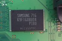
CECHA/COK-001 up to including CECHE/COK-002W : 2x Samsung K9F1G08U0A-PIB0 (NAND 2x1Gbit=256MB total)
CECHG/SEM-001 : 2x Samsung K9F1G08UOB-PIB0 (NAND 2x1Gbit=256MB total)
CECHH/DIA-001 up to including CECHK/DIA-002 : 1x Spansion S29GL128N90TFIR2 (NOR 16MB)
CECHL/VER-001 (1-878-196-31) : 1x Spansion S29GL128P90TFIR2 (NOR 16MB)
CECHL/VER-001 : 1x Spansion S29GL128N90TFIR2 (NOR 16MB)
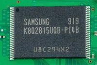
CECHL/VER-001 and PS3 Slim 2... : 1x Samsung K8Q2815UQB-PI4B (NOR 16MB)
CECH-20../DYN-001 (1-880-055-31) : 1x Samsung K8Q2815UQB-PI4B (NOR 16MB)
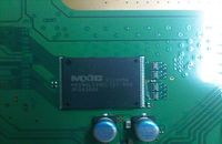
CECH-20../DYN-001 (1-880-055-??) : 1x Macronix MX29GL128ELT2I-90G (NOR Flash)
CECH-20../DYN-001 : 1x Spansion S29GL128P90TFIR2 (NOR Flash)
CECH-250../JTP-001 : 1x Spansion S29GL128P90TFIR2 (NOR 16MB)
CECH-250../JSD-001 : 1x Spansion S29GL128P90TFIR2 (NOR 16MB)
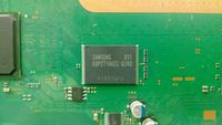
CECH-250../JSD-001 : 1x Samsung K8P2716UZC-QI4D (NOR 16MB)
CECH-30../KTE-001 : 1x Spansion S29GL128P90TFIR2 (NOR 16MB) -OR- 1x Macronix MX29GL128ELT2I-90G (NOR Flash) -OR- 1x Samsung K8P2716UZC-QI4D (NOR Flash)
Non Retail
Reference Tool DECR1000A Communication Processor board : 1x Samsung K9F2G08U0M (NAND 1x2Gbit=256MB total)
Pinout Flash chips
NAND
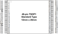
Samsung K9F1G08U0A-PIB0 or K9F1G08UOB-PIB0 (NAND)
productcode meaning:
K - Memory
9 - NAND Flash
F - Small Classification : SLC Normal
1G - Density : 1Gigabit (128MB)
0 - Technology : Normal (x8)
8 - Organisation : x8
U - Vcc Supply Voltage : min 2.7V - Max 3.6V / typ. 3.3V
0 - Mode : Normal
A - Generation : 2nd
-
P - Package : 48pin TSOP1 (12mm x 20mm / 0.5mm pitch)) Lead-free
I - Temperature : Industrial
B - Customer Bad Block : Include Bad Block
0 - PreProgram Version : None
|
|
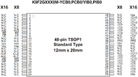
Samsung K9F2G08U0M (NAND)
1x 2 Gbit NAND as used on Reference Tool DECR1000A Communication Processor board
productcode meaning:
K - Memory
9 - NAND Flash
F - Small Classification : SLC Normal
2G - Density : 2Gigabit (256MB)
0 - Technology : Normal (x8)
8 - Organisation : x8
U - Vcc Supply Voltage : min 2.7V - Max 3.6V / typ. 3.3V
0 - Mode : Normal
M - Generation :
-
?P - Package : 48pin TSOP1 (12mm x 20mm / 0.5mm pitch)) Lead-free
?I - Temperature : Industrial
?B - Customer Bad Block : Include Bad Block
?0 - PreProgram Version : None
|
|
NOR
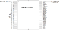
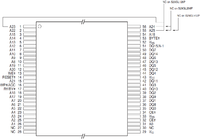
Spansion S29GL128N90TFIR2 (NOR)
productcode meaning:
S29GL128N - 3.0 Volt-only, 512 Megabit (32M x 16-bit/64Mx8-bit), Page-Mode, Flash Memory, 110nm
90 - Speed option : 90ns
T - Package type: TSOP
F - Package materials set : Lead-free
I - Temperature range : Industrial
R2 - ?Vio = 2.7 to 3.6V, lowest address sector protected?
| Pin | Usage | Remarks |
|---|---|---|
| 1 | A23 | No Connection for S29GL128N |
| 2 | A22 | |
| 3 | A15 | |
| 4 | A14 | |
| 5 | A13 | |
| 6 | A12 | |
| 7 | A11 | |
| 8 | A10 | |
| 9 | A9 | |
| 10 | A8 | |
| 11 | A19 | |
| 12 | A20 | |
| 13 | WE# | Write Enable |
| 14 | RESET# | Reset |
| 15 | A21 | |
| 16 | WP#/ACC | Write Protect / Accelerated Program Operation |
| 17 | RD/BY# | Ready/Busy Output |
| 18 | A18 | |
| 19 | A17 | |
| 20 | A7 | |
| 21 | A6 | |
| 22 | A5 | |
| 23 | A4 | |
| 24 | A3 | |
| 25 | A2 | |
| 26 | A1 | |
| 27 | NC | No Connection |
| 28 | NC | No Connection |
| Pin | Usage | Remarks |
|---|---|---|
| 29 | Vio | Vio - Output Buffer Power |
| 30 | NC | No Connection |
| 31 | A0 | |
| 32 | CE# | Chip Enable |
| 33 | VSS | Ground |
| 34 | OE# | Output Enable |
| 35 | DQ0 | |
| 36 | DQ8 | |
| 37 | DQ1 | |
| 38 | DQ9 | |
| 39 | DQ2 | |
| 40 | DQ10 | |
| 41 | DQ3 | |
| 42 | DQ11 | |
| 43 | Vcc | Vcc (min 2.7V-max 3.6V / typ 3.0V) |
| 44 | DQ4 | |
| 45 | DQ12 | |
| 46 | DQ5 | |
| 47 | DQ13 | |
| 48 | DQ6 | *OTP? |
| 49 | DQ14 | |
| 50 | DQ7 | *OTP? |
| 51 | DQ15/A-1 | |
| 52 | VSS | Ground |
| 53 | #BYTE | BYTE# Selects 8-bit or 16-bit mode (NC on Samsung K8Q2815UQB-PI4B NOR) |
| 54 | A16 | |
| 55 | NC | No Connection |
| 56 | A24 | No Connection for S29GL128N and S29GL256N |
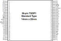
Spansion S29GL128P90TFIR2 (NOR)
productcode meaning:
S29GL128P - 3.0 Volt-only, 512 Megabit (32M x 16-bit/64Mx8-bit), Page-Mode, Flash Memory, 90nm
90 - Speed option : 90ns
T - Package type: TSOP
F - Package materials set : Lead-free
I - Temperature range : Industrial
R2 - ?Vio = 2.7 to 3.6V, lowest address sector protected?
| Pin | Usage | Remarks |
|---|---|---|
| 1 | A23 | No Connection for S29GL128P |
| 2 | A22 | |
| 3 | A15 | |
| 4 | A14 | |
| 5 | A13 | |
| 6 | A12 | |
| 7 | A11 | |
| 8 | A10 | |
| 9 | A9 | |
| 10 | A8 | |
| 11 | A19 | |
| 12 | A20 | |
| 13 | WE# | Write Enable |
| 14 | RESET# | Reset |
| 15 | A21 | |
| 16 | WP#/ACC | Write Protect / Accelerated Program Operation |
| 17 | RY/BY# | Ready/Busy Output |
| 18 | A18 | |
| 19 | A17 | |
| 20 | A7 | |
| 21 | A6 | |
| 22 | A5 | |
| 23 | A4 | |
| 24 | A3 | |
| 25 | A2 | |
| 26 | A1 | |
| 27 | NC | No Connection |
| 28 | NC | No Connection |
| Pin | Usage | Remarks |
|---|---|---|
| 29 | Vio | Vio - Output Buffer Power |
| 30 | NC | No Connection |
| 31 | A0 | |
| 32 | CE# | Chip Enable |
| 33 | VSS | Ground |
| 34 | OE# | Output Enable |
| 35 | DQ0 | |
| 36 | DQ8 | |
| 37 | DQ1 | |
| 38 | DQ9 | |
| 39 | DQ2 | |
| 40 | DQ10 | |
| 41 | DQ3 | |
| 42 | DQ11 | |
| 43 | Vcc | Vcc (min 2.7V-max 3.6V / typ 3.0V) |
| 44 | DQ4 | |
| 45 | DQ12 | |
| 46 | DQ5 | |
| 47 | DQ13 | |
| 48 | DQ6 | *OTP? |
| 49 | DQ14 | |
| 50 | DQ7 | *OTP? |
| 51 | DQ15/A-1 | |
| 52 | VSS | Ground |
| 53 | #BYTE | BYTE# Selects 8-bit or 16-bit mode (NC on Samsung K8Q2815UQB-PI4B NOR) |
| 54 | A16 | |
| 55 | A25 | No Connection for S29GL128P, S29GL256P and S29GL512P |
| 56 | A24 | No Connection for S29GL128P and S29GL256P |
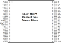
Samsung K8Q2815UQB-PI4B (NOR)
productcode meaning:
K - Memory
8 - NOR Flash
Q - Small Classification : Page Mode DDP
28 - Density : 128M, 8M / 16Bank / 8^8
15 - Dual Bank Boot Block (Bank1, Bank2) : 16M, 2M / 14M
U - Vcc : 3.0V / 3.3V (2.7V~3.6V)
Q - Device Type: Top and Bottom Boot Block
B - Generation : 3rd Generation
-
P - Package : TSOP1 (Lead Free)
I - Temp : Industrial
4B - Speed : 60ns/25ns (Page)
NOTE
Multiple Bank architectures (8 banks)
- Bank 0 : 8Mbit (4Kw x 8 and 32Kw x 15)
- Bank 1 :24Mbit (32Kw x 48)
- Bank 2 : 24Mbit (32Kw x 48)
- Bank 3 : 8Mbit (4Kw x 8 and 32Kw x 15)
- Bank 4 : 8Mbit (4Kw x 8 and 32Kw x 15)
- Bank 5 :24Mbit (32Kw x 48)
- Bank 6 : 24Mbit (32Kw x 48)
- Bank 7 : 8Mbit (4Kw x 8 and 32Kw x 15)
OTP Block : Extra 256 word
- 128word for factory and 128word for customer OTP (only on first Virtual Chip, A22=low)
| Pin | Usage | Remarks |
|---|---|---|
| 1 | NC | No Connection |
| 2 | A22 | Virtual Chip Enable of 2nd Chip |
| 3 | A15 | |
| 4 | A14 | |
| 5 | A13 | |
| 6 | A12 | |
| 7 | A11 | |
| 8 | A10 | |
| 9 | A9 | |
| 10 | A8 | |
| 11 | A19 | |
| 12 | A20 | |
| 13 | WE | Write Enable |
| 14 | RESET | Reset |
| 15 | A21 | |
| 16 | WP/ACC | Write Protect / Accelerated Program Operation |
| 17 | RD/BY | Ready/Busy Output |
| 18 | A18 | |
| 19 | A17 | |
| 20 | A7 | |
| 21 | A6 | |
| 22 | A5 | |
| 23 | A4 | |
| 24 | A3 | |
| 25 | A2 | |
| 26 | A1 | |
| 27 | NC | No Connection |
| 28 | NC | No Connection |
| Pin | Usage | Remarks |
|---|---|---|
| 29 | VCCQ | VccQ |
| 30 | NC | No Connection |
| 31 | A0 | |
| 32 | CE | Chip Enable |
| 33 | VSS | Ground |
| 34 | OE | Output Enable |
| 35 | DQ0 | |
| 36 | DQ8 | |
| 37 | DQ1 | |
| 38 | DQ9 | |
| 39 | DQ2 | |
| 40 | DQ10 | |
| 41 | DQ3 | |
| 42 | DQ11 | |
| 43 | Vcc | Vcc (min 2.7V-max 3.6V / typ 3.0V) |
| 44 | DQ4 | |
| 45 | DQ12 | |
| 46 | DQ5 | |
| 47 | DQ13 | |
| 48 | DQ6 | *OTP? |
| 49 | DQ14 | |
| 50 | DQ7 | *OTP? |
| 51 | DQ15 | |
| 52 | VSS | Ground |
| 53 | NC | No Connection |
| 54 | A16 | |
| 55 | NC | No Connection |
| 56 | NC | No Connection |
- OTP Block Region : 256-word Flash memory region. The data DQ6=1 for customer locked and DQ7=1 for factory locked
Samsung K8P2716UZC-QI4D (NOR)
productcode meaning:
K - Memory
8 - NOR Flash
P
27 - Density : 	128M 	x8/x16
18 - Dual Bank Boot Block :
U - Vcc : 3.0V / 3.3V (2.7V~3.6V)
Z - Device Type:
C - Generation : 4rd Generation
-
Q - Package : 	56TSOP1
I - Temp : Industrial
4D - Speed : 70ns/30ns(Page)
| Pin | Usage | Remarks |
|---|---|---|
| 1 | NC | No Connection |
| 2 | A22 | |
| 3 | A15 | |
| 4 | A14 | |
| 5 | A13 | |
| 6 | A12 | |
| 7 | A11 | |
| 8 | A10 | |
| 9 | A9 | |
| 10 | A8 | |
| 11 | A19 | |
| 12 | A20 | |
| 13 | WE# | Write Enable |
| 14 | RESET# | Reset |
| 15 | A21 | |
| 16 | WP#/ACC | Write Protect / Accelerated Program Operation |
| 17 | RD/BY# | Ready/Busy Output |
| 18 | A18 | |
| 19 | A17 | |
| 20 | A7 | |
| 21 | A6 | |
| 22 | A5 | |
| 23 | A4 | |
| 24 | A3 | |
| 25 | A2 | |
| 26 | A1 | |
| 27 | NC | No Connection |
| 28 | NC | No Connection |
| Pin | Usage | Remarks |
|---|---|---|
| 29 | Vio | Vio - Output Buffer Power |
| 30 | NC | No Connection |
| 31 | A0 | |
| 32 | CE# | Chip Enable |
| 33 | VSS | Ground |
| 34 | OE# | Output Enable |
| 35 | DQ0 | |
| 36 | DQ8 | |
| 37 | DQ1 | |
| 38 | DQ9 | |
| 39 | DQ2 | |
| 40 | DQ10 | |
| 41 | DQ3 | |
| 42 | DQ11 | |
| 43 | Vcc | Vcc (min 2.7V-max 3.6V / typ 3.0V) |
| 44 | DQ4 | |
| 45 | DQ12 | |
| 46 | DQ5 | |
| 47 | DQ13 | |
| 48 | DQ6 | |
| 49 | DQ14 | |
| 50 | DQ7 | |
| 51 | DQ15/A-1 | |
| 52 | VSS | Ground |
| 53 | #BYTE | BYTE# Selects 8-bit or 16-bit mode |
| 54 | A16 | |
| 55 | NC | No Connection |
| 56 | NC | No Connection |
Macronix MX29GL128ELT2I-90G (NOR)
productcode meaning:
MX29GL Series
3V
128 Mb
16M x 8/8M x 16
90ns
Parallel Flash
TSOP-56
| Pin | Usage | Remarks |
|---|---|---|
| 1 | NC | No Connection |
| 2 | A22 | |
| 3 | A15 | |
| 4 | A14 | |
| 5 | A13 | |
| 6 | A12 | |
| 7 | A11 | |
| 8 | A10 | |
| 9 | A9 | |
| 10 | A8 | |
| 11 | A19 | |
| 12 | A20 | |
| 13 | WE# | Write Enable |
| 14 | RESET# | Reset |
| 15 | A21 | |
| 16 | WP#/ACC | Write Protect / Accelerated Program Operation |
| 17 | RD/BY# | Ready/Busy Output |
| 18 | A18 | |
| 19 | A17 | |
| 20 | A7 | |
| 21 | A6 | |
| 22 | A5 | |
| 23 | A4 | |
| 24 | A3 | |
| 25 | A2 | |
| 26 | A1 | |
| 27 | NC | No Connection |
| 28 | NC | No Connection |
| Pin | Usage | Remarks |
|---|---|---|
| 29 | VI/O | Vcc I/O (min 2.7V-max 3.6V / typ 3.0V) |
| 30 | NC | No Connection |
| 31 | A0 | |
| 32 | CE# | Chip Enable |
| 33 | GND | Ground |
| 34 | OE# | Output Enable |
| 35 | Q0 | |
| 36 | Q8 | |
| 37 | Q1 | |
| 38 | Q9 | |
| 39 | Q2 | |
| 40 | Q10 | |
| 41 | Q3 | |
| 42 | Q11 | |
| 43 | Vcc | Vcc (min 2.7V-max 3.6V / typ 3.0V) |
| 44 | Q4 | |
| 45 | Q12 | |
| 46 | Q5 | |
| 47 | Q13 | |
| 48 | Q6 | |
| 49 | Q14 | |
| 50 | Q7 | |
| 51 | Q15/A-1 | Q15 (Word Mode) / LSB addr (Byte Mode) |
| 52 | GND | Ground |
| 53 | BYTE# | Selects 8bits or 16bits mode |
| 54 | A16 | |
| 55 | NC | No Connection |
| 56 | NC | No Connection |
Pinout Other
Renesas HN58X2504TIE (EEPROM)
Note: although edepot&others lists it on the board, I can only find this IC in the sixaxis.
Datasheet
productcode meaning:
H -
N -
5 -
8 - Organisation : x8bit
X -
2 -
5 -
0 -
4 - Density : 4-kbit (512x8bit)
T - Package : 8pin plastic TSSOP (TTP-8DAV)
I - Temp : Industrial (-40 to +85 °C
E - Environment : Lead Free
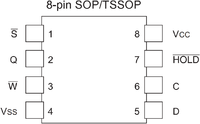
Each PS3 has a special EEPROM chip on the motherboard using a SPI Serial Interface Renasas chip.
| Type | Size | Speed | Voltage | Packaging | Manufacturer | Serial Number | Description |
|---|---|---|---|---|---|---|---|
| EEPROM | 4-kbit (512x8bit) | 3MHz | 1.8V to 5.5V | 8-pin TSSOP | Renesas | HN58X2504TIE | PS3 EEPROM chip |
| Pin | Usage | Remarks |
|---|---|---|
| 1 | S | Chip Select |
| 2 | Q | Serial data output |
| 3 | W | Write Protect |
| 4 | VSS | Ground |
| 5 | D | Serial data input |
| 6 | C | Serial Clock |
| 7 | HOLD | Hold |
| 8 | VCC | Vcc (min 1.8V-max 5.5V) |
