Talk:Switch boards: Difference between revisions
(modding talk) |
mNo edit summary |
||
| Line 2: | Line 2: | ||
== PS3 2000 series Power Eject boards, enabling contour leds talk == | == PS3 2000 series Power Eject boards, enabling contour leds talk == | ||
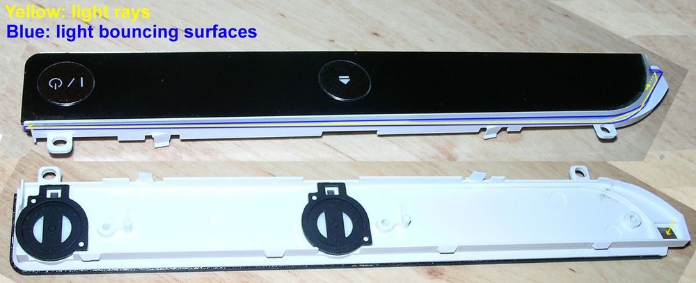
<div style="float:right">[[File:Power Eject board PS3 2000 series (light rays schematic in contour leds).jpg|1000px|thumb|left|Power Eject board PS3 2000 series (light rays schematic in contour leds)]]<BR />[[File:Power Eject board HSW-001 (enabling contour leds).jpg|1000px|thumb|left|Power Eject board HSW-001 (enabling contour leds)]]</div> | <div style="float:right">[[File:Power Eject board PS3 2000 series (light rays schematic in contour leds).jpg|1000px|thumb|left|Power Eject board PS3 2000 series (light rays schematic in contour leds)]]<BR />[[File:Power Eject board HSW-001 (enabling contour leds).jpg|1000px|thumb|left|Power Eject board HSW-001 (enabling contour leds)]]</div> | ||
This is temporal section to discuss the simplest/easyer/safest/better way to make this mod, and the posible variations | This is a temporal section to discuss the simplest/easyer/safest/better way to make this mod, and the posible variations | ||
The photos at the right are a first sketch to discuss how to improve the photos or the circuit | The photos at the right are a first sketch to discuss how to improve the photos or the circuit | ||
| Line 12: | Line 12: | ||
*Circuit squematic photo | *Circuit squematic photo | ||
The cutted trace in pin1 is just because the board was designed to be controlled this way, even if is not in retail models is possible that exist a prototype with it, also is needed to be 100% sure the pin goes nowhere (is posible the trace goes to an internal layer of the | The cutted trace in pin1 is just because the board was designed to be controlled this way, even if is not in retail models is possible that exist a prototype with it, also is needed to be 100% sure the pin goes nowhere (is posible the trace goes to an internal layer of the motherboard not visible in the surface and emerge again in a syscon pin) | ||
The transistor base pin goes in-line with the other unpopulated transistor base pin, both does the same function at the same time, each of this transistors is in chargue of 2 leds. This transistors are "isolating" the subcircuit of the 4 leds | The transistor base pin goes in-line with the other unpopulated transistor base pin, both does the same function at the same time, each of this transistors is in chargue of 2 leds. This transistors are "isolating" the subcircuit of the 4 leds | ||
The unpopulated resistors values are dependant of the leds added, so no need to add the values to the drawing | The unpopulated resistors values are dependant of the leds added, so no need to add the values to the drawing | ||
Revision as of 03:45, 3 July 2013
PS3 2000 series Power Eject boards, enabling contour leds talk
This is a temporal section to discuss the simplest/easyer/safest/better way to make this mod, and the posible variations
The photos at the right are a first sketch to discuss how to improve the photos or the circuit
- Light rays bouncing photo (this goes first because is easy to discuss)
- I could not find a better one where the first bouncing surface is more visible, this first surface is the most important but also the curve for the next bounces, is good to cover this with a mirror sticker (by sticking it in the case, this way the glue layer is at the other side)... no photo of this sticker
- Is barelly visible the light ray starts in verticall, and after the first bounce is in horizontal... arrows didnt helped
- Circuit squematic photo
The cutted trace in pin1 is just because the board was designed to be controlled this way, even if is not in retail models is possible that exist a prototype with it, also is needed to be 100% sure the pin goes nowhere (is posible the trace goes to an internal layer of the motherboard not visible in the surface and emerge again in a syscon pin)
The transistor base pin goes in-line with the other unpopulated transistor base pin, both does the same function at the same time, each of this transistors is in chargue of 2 leds. This transistors are "isolating" the subcircuit of the 4 leds
The unpopulated resistors values are dependant of the leds added, so no need to add the values to the drawing
