Template:Syscon pinout LQFP 100 pins: Difference between revisions
Jump to navigation
Jump to search
(RSX_CGRST better explained this way) |
No edit summary |
||
| Line 8: | Line 8: | ||
{|class="wikitable sortable" style="width:100%; line-height:120%; font-size:90%" | {|class="wikitable sortable" style="width:100%; line-height:120%; font-size:90%" | ||
|+ {{captionlinks|Syscon pinout LQFP 100 pins}} | |+ {{captionlinks|Syscon pinout LQFP 100 pins}} | ||
! rowspan="2" style="width:35px; min-width:35px; padding:0px; background-position:50% 88%" | Pin !! rowspan="2" style="width:35px; min-width:35px; padding:0px; background-position:50% 88%" | Port !! colspan="2" class="unsortable" | Name !! rowspan="2" class="unsortable" style="padding:0px" | Type !! rowspan="2" class="unsortable" | Description !! | ! rowspan="2" style="width:35px; min-width:35px; padding:0px; background-position:50% 88%" | Pin !! rowspan="2" style="width:35px; min-width:35px; padding:0px; background-position:50% 88%" | Port !! colspan="2" class="unsortable" | Name !! rowspan="2" class="unsortable" style="padding:0px" | Type !! rowspan="2" class="unsortable" | Description !! colspan="2" style="width:50px;" class="unsortable" | Voltages | ||
|- | |- | ||
! class="unsortable" | <abbr title="NEC/Renesas optional pin configuration">NEC/Renesas</abbr> !! class="unsortable" | Sony/Custom | ! class="unsortable" | <abbr title="NEC/Renesas optional pin configuration">NEC/Renesas</abbr> !! class="unsortable" | Sony/Custom !! class="unsortable" | <abbr title="Standby">Stby</abbr> !! class="unsortable" | <abbr title="Running">Runn</abbr> | ||
|- | |- | ||
| 1 || 14 || {{cellcolors|#77f|#ff0}} SCL20 || HDMI_I2C_SCL || {{pino}} || Connected to [[HDMI]] controller [[MN8647091]] pin 27 || 0 | | 1 || 14 || {{cellcolors|#77f|#ff0}} SCL20 || HDMI_I2C_SCL || {{pino}} || Connected to [[HDMI]] controller [[MN8647091]] pin 27 || 0 || | ||
|- | |- | ||
| 2 || 14 || P141/PCLBUZ1/INTP7 || SB_RESET ?, or SB_CGRST ? || ←I/O→ || Connected to [[South Bridge]] [[CXD9963GB]] pad AA17 || | | 2 || 14 || P141/PCLBUZ1/INTP7 || SB_RESET ?, or SB_CGRST ? || ←I/O→ || Connected to [[South Bridge]] [[CXD9963GB]] pad AA17 || || | ||
|- | |- | ||
| 3 || 14 || P140/PCLBUZ0/INTP6 || || ←I/O→ || Connected to [[South Bridge]] [[CXD9963GB]] pad W22 || | | 3 || 14 || P140/PCLBUZ0/INTP6 || || ←I/O→ || Connected to [[South Bridge]] [[CXD9963GB]] pad W22 || || | ||
|- | |- | ||
| 4 || 12 || P120/INTP0/EXLVI || || ←I/O→ || External potential input for low-voltage detector ? || 1.5V | | 4 || 12 || P120/INTP0/EXLVI || || ←I/O→ || External potential input for low-voltage detector ? || || 1.5V | ||
|- | |- | ||
| 5 || 4 || P47/INTP2 || || ←I/O→ || BT_WAKEON ??? Connected to Wifi/BT module ??? (BT_WAKEON ? or BT_RESET ?) || | | 5 || 4 || P47/INTP2 || || ←I/O→ || BT_WAKEON ??? Connected to Wifi/BT module ??? (BT_WAKEON ? or BT_RESET ?) || || | ||
|- | |- | ||
| 6 || 4 || {{cellcolors|#246|#fff}} TO05 || BUZZER || {{pino}} || Connected to the Buzzer through a transistor || | | 6 || 4 || {{cellcolors|#246|#fff}} TO05 || BUZZER || {{pino}} || Connected to the Buzzer through a transistor || || | ||
|- | |- | ||
| 7 || 4 || P45/SO01 || || ←I/O→ || Connected to pin 11 bdrom IC || 3.3V | | 7 || 4 || P45/SO01 || || ←I/O→ || Connected to pin 11 bdrom IC || || 3.3V | ||
|- | |- | ||
| 8 || 4 || P44/SI01 || || ←I/O→ || Connected to pin 22 isl IC || 3.3V | | 8 || 4 || P44/SI01 || || ←I/O→ || Connected to pin 22 isl IC || 3.3V || 3.3V | ||
|- | |- | ||
| 9 || 4 || P43/<span style="text-decoration: overline;">SCK01</span> || || ←I/O→ || Connected to pin 23 isl IC || 3.3V | | 9 || 4 || P43/<span style="text-decoration: overline;">SCK01</span> || || ←I/O→ || Connected to pin 23 isl IC || 3.3V || 3.3V | ||
|- | |- | ||
| 10 || 4 || P42/TI04/TO04 || SB_RESET ?, or SB_CGRST ? || ←I/O→ || Connected to [[South Bridge]] [[CXD9963GB]] pad AA18 | | 10 || 4 || P42/TI04/TO04 || SB_RESET ?, or SB_CGRST ? || ←I/O→ || Connected to [[South Bridge]] [[CXD9963GB]] pad AA18 | ||
|| 3.3V | || || 3.3V | ||
|- | |- | ||
| 11 || 4 || {{cellcolors|#a74}} TOOL1 || TOOL_CLK || ? || Connected to [[Service_Connectors#CN.3F.3F.3F.3F|Service Connector 3rd Gen.]] pin 13 (Tool clock) through a missing resistor ? || 3.3V | | 11 || 4 || {{cellcolors|#a74}} TOOL1 || TOOL_CLK || ? || Connected to [[Service_Connectors#CN.3F.3F.3F.3F|Service Connector 3rd Gen.]] pin 13 (Tool clock) through a missing resistor ? || || 3.3V | ||
|- | |- | ||
| 12 || 4 || {{cellcolors|#a74}} TOOL0 || TOOL_DAT || {{pinio}} || Connected to [[Service_Connectors#CN.3F.3F.3F.3F|Service Connector 3rd Gen.]] pin 7 (Tool Data) through a missing resistor ? || 3.3V | | 12 || 4 || {{cellcolors|#a74}} TOOL0 || TOOL_DAT || {{pinio}} || Connected to [[Service_Connectors#CN.3F.3F.3F.3F|Service Connector 3rd Gen.]] pin 7 (Tool Data) through a missing resistor ? || || 3.3V | ||
|- | |- | ||
| 13 || data-sort-value="17"| || {{cellcolors|#a74}} <span style="text-decoration: overline;">RESET</span> || RST || {{pini}} || || 3.3V | | 13 || data-sort-value="17"| || {{cellcolors|#a74}} <span style="text-decoration: overline;">RESET</span> || RST || {{pini}} || || || 3.3V | ||
|- | |- | ||
| 14 || 12 || {{cellcolors|#555|#fff}} XT2 || OSCOUT || {{pino}} || Subsystem clock. Connected to a big black crystal. Amplitude (32.768Khz?) || 1.2V | | 14 || 12 || {{cellcolors|#555|#fff}} XT2 || OSCOUT || {{pino}} || Subsystem clock. Connected to a big black crystal. Amplitude (32.768Khz?) || 1.2V || 1.2V | ||
|- | |- | ||
| 15 || 12 || {{cellcolors|#555|#fff}} XT1 || OSCIN || {{pini}} || Subsystem clock. Connected to a big black crystal. Amplitude (32.768Khz?) || 0. | | 15 || 12 || {{cellcolors|#555|#fff}} XT1 || OSCIN || {{pini}} || Subsystem clock. Connected to a big black crystal. Amplitude (32.768Khz?) || || 0.8V | ||
|- | |- | ||
| 16 || data-sort-value="17"| || {{cellcolors|#a74}} FLMD0 || FLASH_MODE || {{pini}} || || 3.3V | | 16 || data-sort-value="17"| || {{cellcolors|#a74}} FLMD0 || FLASH_MODE || {{pini}} || || 3.3V || 3.3V | ||
|- | |- | ||
| 17 || 12 || {{cellcolors|#555|#fff}} X2 || XTAL || {{pino}} || Main system clock. Connected to a white ceramic crystal marked "ED" or "EU" || | | 17 || 12 || {{cellcolors|#555|#fff}} X2 || XTAL || {{pino}} || Main system clock. Connected to a white ceramic crystal marked "ED" or "EU" || || | ||
|- | |- | ||
| 18 || 12 || {{cellcolors|#555|#fff}} X1 || EXTAL || {{pini}} || Main system clock. Connected to a white ceramic crystal marked "ED" or "EU" || | | 18 || 12 || {{cellcolors|#555|#fff}} X1 || EXTAL || {{pini}} || Main system clock. Connected to a white ceramic crystal marked "ED" or "EU" || || | ||
|- | |- | ||
| 19 || data-sort-value="18"| || {{cellcolors|#f93}} REGC || VREG_CAP || {{pin}} || || 2.5V | | 19 || data-sort-value="18"| || {{cellcolors|#f93}} REGC || VREG_CAP || {{pin}} || || || 2.5V | ||
|- | |- | ||
| 20 || data-sort-value="20"| || {{cellcolors|#333|#fff}} V<span style="font-size:60%;">SS</span> || GND || {{pin}} || || | | 20 || data-sort-value="20"| || {{cellcolors|#333|#fff}} V<span style="font-size:60%;">SS</span> || GND || {{pin}} || || || | ||
|- | |- | ||
| 21 || data-sort-value="20"| || {{cellcolors|#333|#fff}} EV<span style="font-size:60%;">SS0</span> || GND || {{pin}} || || | | 21 || data-sort-value="20"| || {{cellcolors|#333|#fff}} EV<span style="font-size:60%;">SS0</span> || GND || {{pin}} || || || | ||
|- | |- | ||
| 22 || data-sort-value="19"| || {{cellcolors|#f33|#fff}} V<span style="font-size:60%;">DD</span> || 3.3_EVER_B || {{pin}} || || 3.3V | | 22 || data-sort-value="19"| || {{cellcolors|#f33|#fff}} V<span style="font-size:60%;">DD</span> || 3.3_EVER_B || {{pin}} || || 3.3V || 3.3V | ||
|- | |- | ||
| 23 || data-sort-value="19"| || {{cellcolors|#f33|#fff}} EV<span style="font-size:60%;">DD0</span> || 3.3_EVER_B || {{pin}} || || 3.3V | | 23 || data-sort-value="19"| || {{cellcolors|#f33|#fff}} EV<span style="font-size:60%;">DD0</span> || 3.3_EVER_B || {{pin}} || || 3.3V || 3.3V | ||
|- | |- | ||
| 24 || 6 || P60/SCL0 || MK_I2C_SCL ? || ←I/O→ || Connected to Texas Instruments-SCEI Clock Generator CDC972 pin 37 ??? || | | 24 || 6 || P60/SCL0 || MK_I2C_SCL ? || ←I/O→ || Connected to Texas Instruments-SCEI Clock Generator CDC972 pin 37 ??? || || | ||
|- | |- | ||
| 25 || 6 || P61/SDA0 || MK_I2C_SDA ? || ←I/O→ || Connected to Texas Instruments-SCEI Clock Generator CDC972 pin 38 ??? || | | 25 || 6 || P61/SDA0 || MK_I2C_SDA ? || ←I/O→ || Connected to Texas Instruments-SCEI Clock Generator CDC972 pin 38 ??? || || | ||
|- | |- | ||
! style="padding:0px" data-sort-value="25.5"| || style="padding:0px" data-sort-value="0.5"| || style="padding:0px" colspan=" | ! style="padding:0px" data-sort-value="25.5"| || style="padding:0px" data-sort-value="0.5"| || style="padding:0px" colspan="6" | | ||
|- | |- | ||
! style="padding:0px" data-sort-value="25.5"| || style="padding:0px" data-sort-value="1.5"| || style="padding:0px" colspan=" | ! style="padding:0px" data-sort-value="25.5"| || style="padding:0px" data-sort-value="1.5"| || style="padding:0px" colspan="6" | | ||
|- | |- | ||
! style="padding:0px" data-sort-value="25.5"| || style="padding:0px" data-sort-value="2.5"| || style="padding:0px" colspan=" | ! style="padding:0px" data-sort-value="25.5"| || style="padding:0px" data-sort-value="2.5"| || style="padding:0px" colspan="6" | | ||
|- | |- | ||
! style="padding:0px" data-sort-value="25.5"| || style="padding:0px" data-sort-value="3.5"| || style="padding:0px" colspan=" | ! style="padding:0px" data-sort-value="25.5"| || style="padding:0px" data-sort-value="3.5"| || style="padding:0px" colspan="6" | | ||
|- | |- | ||
! style="padding:0px" data-sort-value="25.5"| || style="padding:0px" data-sort-value="4.5"| || style="padding:0px" colspan=" | ! style="padding:0px" data-sort-value="25.5"| || style="padding:0px" data-sort-value="4.5"| || style="padding:0px" colspan="6" | | ||
|- | |- | ||
| 26 || 6 || P62 || || ←I/O→ || Connected to pin 3 isl ic || 2.5V | | 26 || 6 || P62 || || ←I/O→ || Connected to pin 3 isl ic || || 2.5V | ||
|- | |- | ||
| 27 || 6 || P63 || || ←I/O→ || 10K resistor to GND ? || 3.3V | | 27 || 6 || P63 || || ←I/O→ || 10K resistor to GND ? || 3.3V || | ||
|- | |- | ||
| 28 || 3 || P31/TI03/TO03/INTP4 || ACIN_DET ? || ←I/O→ || pin 4 to wifi5v vreg ic/EN ? | | 28 || 3 || P31/TI03/TO03/INTP4 || ACIN_DET ? || ←I/O→ || pin 4 to wifi5v vreg ic/EN ? | ||
|| | || || | ||
|- | |- | ||
| 29 || 6 || P64/<span style="text-decoration: overline;">RD</span> || || ←I/O→ || Connected (indirectly) to a voltage regulator ? (to enable something ?) || 3.3V | | 29 || 6 || P64/<span style="text-decoration: overline;">RD</span> || || ←I/O→ || Connected (indirectly) to a voltage regulator ? (to enable something ?) || || 3.3V | ||
|- | |- | ||
| 30 || 6 || P65/<span style="text-decoration: overline;">WR0</span> || || ←I/O→ || Connected to the service connector ? / ic idt4227 pin1 | | 30 || 6 || P65/<span style="text-decoration: overline;">WR0</span> || || ←I/O→ || Connected to the service connector ? / ic idt4227 pin1 | ||
|| 3.3V | || || 3.3V | ||
|- | |- | ||
| 31 || 6 || P66/<span style="text-decoration: overline;">WR1</span> || || ←I/O→ || connected to cdc750 ic pin 33 | | 31 || 6 || P66/<span style="text-decoration: overline;">WR1</span> || || ←I/O→ || connected to cdc750 ic pin 33 | ||
|| 3.3V | || || 3.3V | ||
|- | |- | ||
| 32 || 6 || P67/ASTB || NOT_CONNECTED ? || ←I/O→ || connected to cdc750 ic pin 34 | | 32 || 6 || P67/ASTB || NOT_CONNECTED ? || ←I/O→ || connected to cdc750 ic pin 34 | ||
|| 3.3V | || || 3.3V | ||
|- | |- | ||
| 33 || 7 || P77/EX23/KR7/INTP11 || || ←I/O→ || connected to bd3527 pin12(usb side) | | 33 || 7 || P77/EX23/KR7/INTP11 || || ←I/O→ || connected to bd3527 pin12(usb side) | ||
|| 3.3V | || || 3.3V | ||
|- | |- | ||
| 34 || 7 || P76/EX22/KR6/INTP10 || || ←I/O→ || connected to isl6331 pin24 | | 34 || 7 || P76/EX22/KR6/INTP10 || || ←I/O→ || connected to isl6331 pin24 | ||
|| 3.3V | || || 3.3V | ||
|- | |- | ||
| 35 || 7 || P75/EX21/KR5/INTP9 || || ←I/O→ || Connected to [[South Bridge]] [[CXD9963GB]] pad U19 throught 4k7 resistor || 3.3V | | 35 || 7 || P75/EX21/KR5/INTP9 || || ←I/O→ || Connected to [[South Bridge]] [[CXD9963GB]] pad U19 throught 4k7 resistor | ||
|| || 3.3V | |||
|- | |- | ||
| 36 || 7 || P74/EX20/KR4/INTP8 || || ←I/O→ || 10K resistor to GND ? / connected to isl6331 pin20 || 3.3V | | 36 || 7 || P74/EX20/KR4/INTP8 || || ←I/O→ || 10K resistor to GND ? / connected to isl6331 pin20 | ||
|| || 3.3V | |||
|- | |- | ||
| 37 || 7 || P73/EX19/KR3 || || ←I/O→ || Connected to the service connector pin3 / pin 6 ic D35236SK || 3.3V | | 37 || 7 || P73/EX19/KR3 || || ←I/O→ || Connected to the service connector pin3 / pin 6 ic D35236SK | ||
|| || 3.3V | |||
|- | |- | ||
| 38 || 7 || P72/EX18/KR2 || || ←I/O→ || Connected to pin7 ic D35326SK || 3.3V | | 38 || 7 || P72/EX18/KR2 || || ←I/O→ || Connected to pin7 ic D35326SK | ||
|| || 3.3V | |||
|- | |- | ||
| 39 || 7 || P71/EX17/KR1 || || ←I/O→ || Connected to a voltage regulator ? (to enable something ?) / pin11 ic 35255 (top side test nor-pads) | | 39 || 7 || P71/EX17/KR1 || || ←I/O→ || Connected to a voltage regulator ? (to enable something ?) / pin11 ic 35255 (top side test nor-pads) | ||
|| 3.3V | || || 3.3V | ||
|- | |- | ||
| 40 || 7 || P70/EX16/KR0 || || ←I/O→ || Connected to pin10 ic PS 53123 | | 40 || 7 || P70/EX16/KR0 || || ←I/O→ || Connected to pin10 ic PS 53123 | ||
|| 3.3V | || || 3.3V | ||
|- | |- | ||
| 41 || 0 || P06/<span style="text-decoration: overline;">WAIT</span> || || ←I/O→ || 45K resistor to GND ?/ Connected to pin7 ic PS 53123 | | 41 || 0 || P06/<span style="text-decoration: overline;">WAIT</span> || || ←I/O→ || 45K resistor to GND ?/ Connected to pin7 ic PS 53123 | ||
|| | || || | ||
|- | |- | ||
| 42 || 0 || P05/CLKOUT || || ←I/O→ || 45K resistor to GND ? / Connected to pin17 ic PS 53123 | | 42 || 0 || P05/CLKOUT || || ←I/O→ || 45K resistor to GND ? / Connected to pin17 ic PS 53123 | ||
|| 3.3V | || || 3.3V | ||
|- | |- | ||
| 43 || data-sort-value="20"| || {{cellcolors|#333|#fff}} EV<span style="font-size:60%;">SS1</span> || GND || {{pin}} || || | | 43 || data-sort-value="20"| || {{cellcolors|#333|#fff}} EV<span style="font-size:60%;">SS1</span> || GND || {{pin}} || | ||
|| || | |||
|- | |- | ||
| 44 || 8 || P80/EX0 || || ←I/O→ || pull up to 3v3 | | 44 || 8 || P80/EX0 || || ←I/O→ || pull up to 3v3 | ||
|| | || || | ||
|- | |- | ||
| 45 || 8 || P81/EX1 || || ←I/O→ || 1 ohm resistor to ground / pull down to gnd 0 ohms | | 45 || 8 || P81/EX1 || || ←I/O→ || 1 ohm resistor to ground / pull down to gnd 0 ohms | ||
| Line 126: | Line 131: | ||
|- | |- | ||
| 46 || 8 || P82/EX2 || || ←I/O→ || pin 95 hdmi ic | | 46 || 8 || P82/EX2 || || ←I/O→ || pin 95 hdmi ic | ||
|| 3.3V | || || 3.3V | ||
|- | |- | ||
| 47 || 8 || P83/EX3 || || ←I/O→ || 1 ohm resistor to ground / pull down to gnd 0 ohms | | 47 || 8 || P83/EX3 || || ←I/O→ || 1 ohm resistor to ground / pull down to gnd 0 ohms | ||
| Line 132: | Line 137: | ||
|- | |- | ||
| 48 || 8 || P84/EX4 || || ←I/O→ || Connected to pin1 EN vreg 8D11 (bottom side of power pcb) | | 48 || 8 || P84/EX4 || || ←I/O→ || Connected to pin1 EN vreg 8D11 (bottom side of power pcb) | ||
|| 3.3V | || || 3.3V | ||
|- | |- | ||
| 49 || 8 || P85/EX5 || || ←I/O→ || Connected to pin3 ic PS 53123 | | 49 || 8 || P85/EX5 || || ←I/O→ || Connected to pin3 ic PS 53123 | ||
|| 3.3V | || || 3.3V | ||
|- | |- | ||
| 50 || 8 || P86/EX6 || || ←I/O→ || Connected to ic idt4227 pin12 | | 50 || 8 || P86/EX6 || || ←I/O→ || Connected to ic idt4227 pin12 | ||
|| 3.3V | || || 3.3V | ||
|- | |- | ||
! style="padding:0px" data-sort-value="50.5"| || style="padding:0px" data-sort-value="5.5"| || style="padding:0px" colspan=" | ! style="padding:0px" data-sort-value="50.5"| || style="padding:0px" data-sort-value="5.5"| || style="padding:0px" colspan="6" | | ||
|- | |- | ||
! style="padding:0px" data-sort-value="50.5"| || style="padding:0px" data-sort-value="6.5"| || style="padding:0px" colspan=" | ! style="padding:0px" data-sort-value="50.5"| || style="padding:0px" data-sort-value="6.5"| || style="padding:0px" colspan="6" | | ||
|- | |- | ||
! style="padding:0px" data-sort-value="50.5"| || style="padding:0px" data-sort-value="7.5"| || style="padding:0px" colspan=" | ! style="padding:0px" data-sort-value="50.5"| || style="padding:0px" data-sort-value="7.5"| || style="padding:0px" colspan="6" | | ||
|- | |- | ||
! style="padding:0px" data-sort-value="50.5"| || style="padding:0px" data-sort-value="10.5"| || style="padding:0px" colspan=" | ! style="padding:0px" data-sort-value="50.5"| || style="padding:0px" data-sort-value="10.5"| || style="padding:0px" colspan="6" | | ||
|- | |- | ||
! style="padding:0px" data-sort-value="50.5"| || style="padding:0px" data-sort-value="11.5"| || style="padding:0px" colspan=" | ! style="padding:0px" data-sort-value="50.5"| || style="padding:0px" data-sort-value="11.5"| || style="padding:0px" colspan="6" | | ||
|- | |- | ||
| 51 || 8 || P87/EX7 || || ←I/O→ || Connected to power pcb connector | | 51 || 8 || P87/EX7 || || ←I/O→ || Connected to power pcb connector | ||
|| 3.3V | || || 3.3V | ||
|- | |- | ||
| 52 || 3 || P30/INTP3/RTC1HZ || || ←I/O→ || Connected to isl6331 pin21 | | 52 || 3 || P30/INTP3/RTC1HZ || || ←I/O→ || Connected to isl6331 pin21 | ||
|| 3.3V | || || 3.3V | ||
|- | |- | ||
| 53 || data-sort-value="19"| || {{cellcolors|#f33|#fff}} EV<span style="font-size:60%;">DD1</span> || 3.3_EVER_B || {{pin}} || || 3.3V | | 53 || data-sort-value="19"| || {{cellcolors|#f33|#fff}} EV<span style="font-size:60%;">DD1</span> || 3.3_EVER_B || {{pin}} || | ||
|| 3.3V || 3.3V | |||
|- | |- | ||
| 54 || 5 || P50/EX8 || || ←I/O→ || Connected to isl6331 pin25 | | 54 || 5 || P50/EX8 || || ←I/O→ || Connected to isl6331 pin25 | ||
|| 3.3V | || || 3.3V | ||
|- | |- | ||
| 55 || 5 || P51/EX9 || || ←I/O→ || Connected to [[South Bridge]] [[CXD9963GB]] pad W21. And in line 10k to gnd || | | 55 || 5 || P51/EX9 || || ←I/O→ || Connected to [[South Bridge]] [[CXD9963GB]] pad W21. And in line 10k to gnd || || | ||
|- | |- | ||
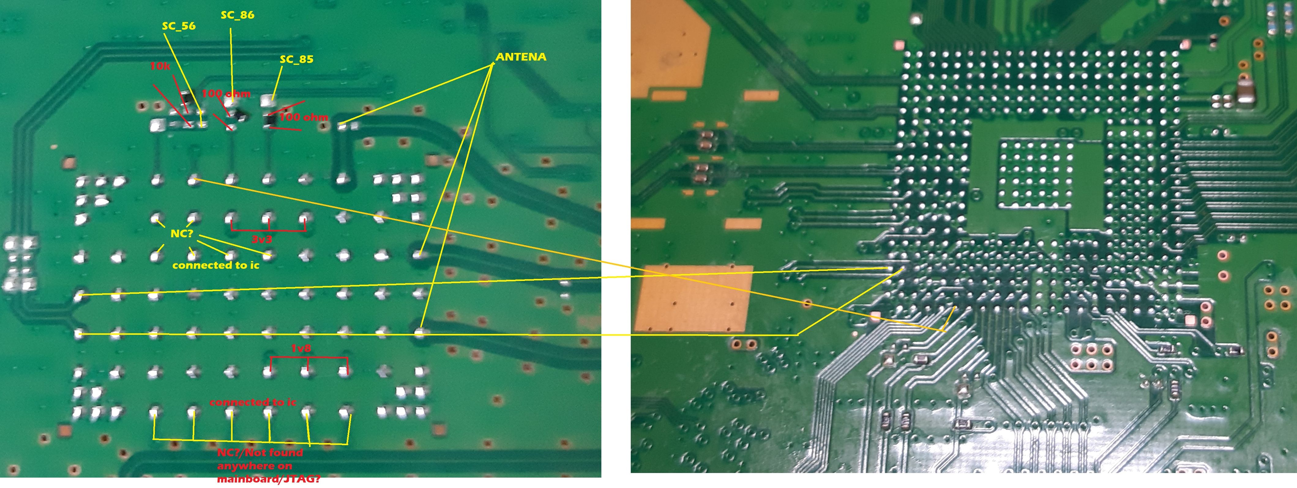
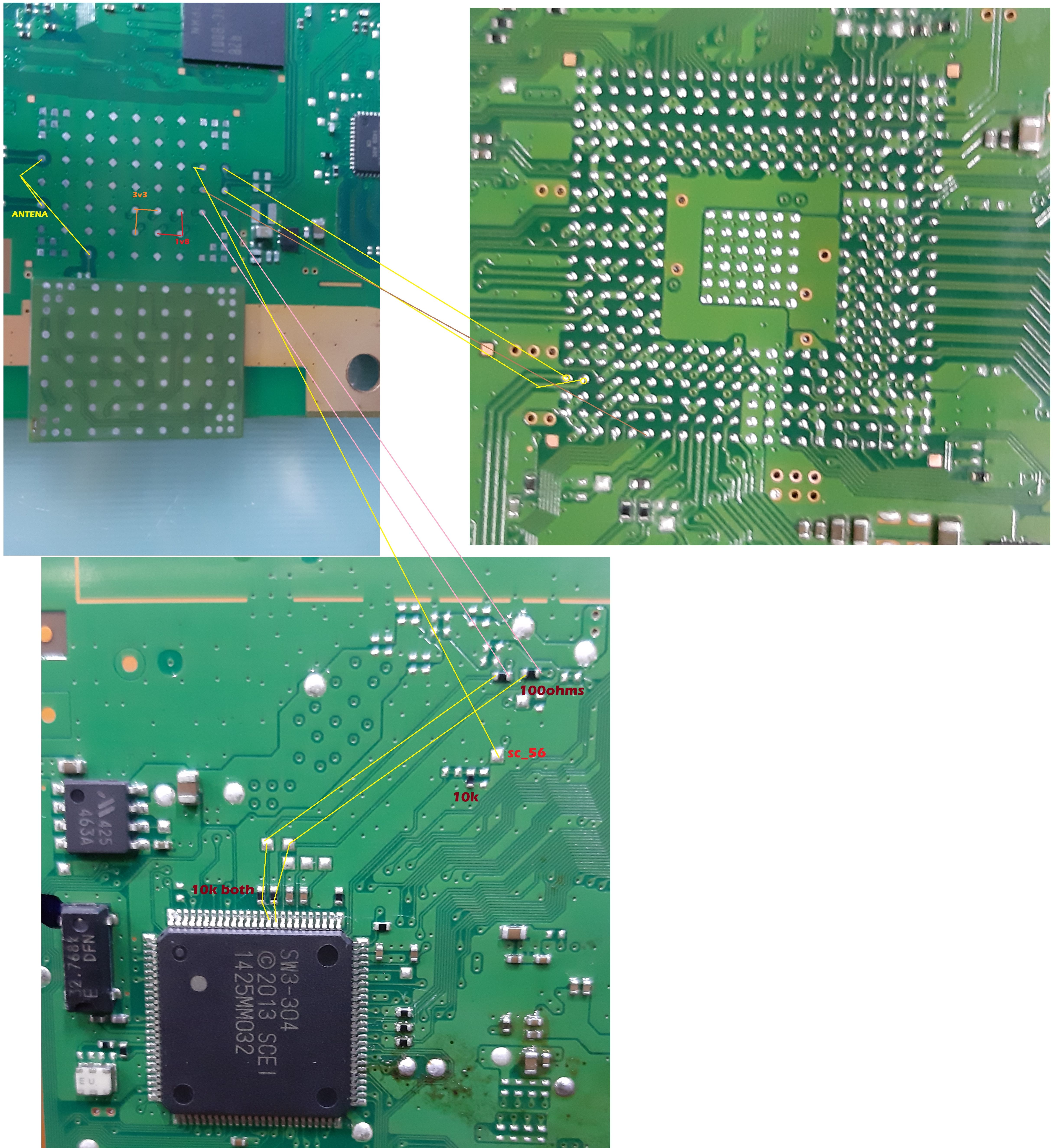
| 56 || 5 || {{cellcolors|#d9f|#fff}} P52/EX10 || WIFI_CTRL || ←I/O→ || 10k resistor to GND, and to wifi/BT module. See: [[Media:KTE-001_wifitraces.jpg|wifi/BT 10x7 pinout]] or [[Media:REX-001_wifitraces.jpg|wifi/BT 9x7 pinout]] || | | 56 || 5 || {{cellcolors|#d9f|#fff}} P52/EX10 || WIFI_CTRL || ←I/O→ || 10k resistor to GND, and to wifi/BT module. See: [[Media:KTE-001_wifitraces.jpg|wifi/BT 10x7 pinout]] or [[Media:REX-001_wifitraces.jpg|wifi/BT 9x7 pinout]] || Vary || 3.3V | ||
|- | |- | ||
| 57 || 5 || {{cellcolors|#a74}} P53 || UART0_RxD || {{pini}} || Syscon UART. Connected to service connector ? || | | 57 || 5 || {{cellcolors|#a74}} P53 || UART0_RxD || {{pini}} || Syscon UART. Connected to service connector ? || || | ||
|- | |- | ||
| 58 || 5 || {{cellcolors|#a74}} P54 || UART0_TxD || {{pino}} || Syscon UART. Connected to service connector ? || | | 58 || 5 || {{cellcolors|#a74}} P54 || UART0_TxD || {{pino}} || Syscon UART. Connected to service connector ? || Vary || 3.3V | ||
|- | |- | ||
| 59 || 5 || P55/EX13 || || ←I/O→ || Connected to [[South Bridge]] [[CXD9963GB]] pad S19 || 3.3V | | 59 || 5 || P55/EX13 || || ←I/O→ || Connected to [[South Bridge]] [[CXD9963GB]] pad S19 || || 3.3V | ||
|- | |- | ||
| 60 || 5 || P56/EX14 || || ←I/O→ || Connected to [[South Bridge]] [[CXD9963GB]] pad V22. And in line 47ohms (SB_INT?) || 3.3V | | 60 || 5 || P56/EX14 || || ←I/O→ || Connected to [[South Bridge]] [[CXD9963GB]] pad V22. And in line 47ohms (SB_INT?) || || 3.3V | ||
|- | |- | ||
| 61 || 5 || P57/EX15 || || ←I/O→ || Connected to [[South Bridge]] [[CXD9963GB]] pad U18 || 3.3V | | 61 || 5 || P57/EX15 || || ←I/O→ || Connected to [[South Bridge]] [[CXD9963GB]] pad U18 || || 3.3V | ||
|- | |- | ||
| 62 || 1 || {{cellcolors|#33f|#e77}} P17/EX31/TI02/TO02 || RSX_VINTE0/VD_VINT0 || {{pini}} || Connected to [[RSX]] pad AR22 ([[Template:RSX pad layout 41x41|RSX layout 41x41]]), or pad <abbr title="Unknown>UNK</abbr> ([[Template:RSX_pad_layout_34x34|RSX layout 34x34]]) through a 10k resistor || 1.5V | | 62 || 1 || {{cellcolors|#33f|#e77}} P17/EX31/TI02/TO02 || RSX_VINTE0/VD_VINT0 || {{pini}} || Connected to [[RSX]] pad AR22 ([[Template:RSX pad layout 41x41|RSX layout 41x41]]), or pad <abbr title="Unknown>UNK</abbr> ([[Template:RSX_pad_layout_34x34|RSX layout 34x34]]) through a 10k resistor || || 1.5V | ||
|- | |- | ||
| 63 || 1 || {{cellcolors|#33f|#e77}} P16/EX30/TI01/TO01/INTP5 || RSX_CGRST || {{pinnc}} || <strike>Connected to [[RSX]] pad AV6 ([[Template:RSX pad layout 41x41|RSX layout 41x41]]), or pad <abbr title="Unknown>UNK</abbr> ([[Template:RSX_pad_layout_34x34|RSX layout 34x34]])</strike><br>This pin is "nerfed" with a 10k resistor to GND in RSX41x41 pad AV6 so syscon is not able to RESET the RSX CG || 0.8V | | 63 || 1 || {{cellcolors|#33f|#e77}} P16/EX30/TI01/TO01/INTP5 || RSX_CGRST || {{pinnc}} || <strike>Connected to [[RSX]] pad AV6 ([[Template:RSX pad layout 41x41|RSX layout 41x41]]), or pad <abbr title="Unknown>UNK</abbr> ([[Template:RSX_pad_layout_34x34|RSX layout 34x34]])</strike><br>This pin is "nerfed" with a 10k resistor to GND in RSX41x41 pad AV6 so syscon is not able to RESET the RSX CG || || 0.8V | ||
|- | |- | ||
| 64 || 1 || {{cellcolors|#33f|#e77}} P15/EX29/RTCDIV/RTCCL || RSX_VINTE1/VD_VINT1 || {{pini}} || Connected to [[RSX]] pad AL38 ([[Template:RSX pad layout 41x41|RSX layout 41x41]]), or pad <abbr title="Unknown>UNK</abbr> ([[Template:RSX_pad_layout_34x34|RSX layout 34x34]]) || 1.5V | | 64 || 1 || {{cellcolors|#33f|#e77}} P15/EX29/RTCDIV/RTCCL || RSX_VINTE1/VD_VINT1 || {{pini}} || Connected to [[RSX]] pad AL38 ([[Template:RSX pad layout 41x41|RSX layout 41x41]]), or pad <abbr title="Unknown>UNK</abbr> ([[Template:RSX_pad_layout_34x34|RSX layout 34x34]]) || || 1.5V | ||
|- | |- | ||
| 65 || 1 || {{cellcolors|#33f|#e77}} P14/EX28 || RSX_RESET || {{pino}} || Connected to [[RSX]] pad AW5 ([[Template:RSX pad layout 41x41|RSX layout 41x41]]), or pad <abbr title="Unknown>UNK</abbr> ([[Template:RSX_pad_layout_34x34|RSX layout 34x34]]) || 1.5V | | 65 || 1 || {{cellcolors|#33f|#e77}} P14/EX28 || RSX_RESET || {{pino}} || Connected to [[RSX]] pad AW5 ([[Template:RSX pad layout 41x41|RSX layout 41x41]]), or pad <abbr title="Unknown>UNK</abbr> ([[Template:RSX_pad_layout_34x34|RSX layout 34x34]]) || || 1.5V | ||
|- | |- | ||
| 66 || 1 || {{cellcolors|#33f|#fff}} P13 || RSX_SPI_CS || {{pino}} || Connected to [[RSX]] pad AW8 ([[Template:RSX pad layout 41x41|RSX layout 41x41]]), or pad <abbr title="Unknown>UNK</abbr> ([[Template:RSX_pad_layout_34x34|RSX layout 34x34]]) || 1.5V | | 66 || 1 || {{cellcolors|#33f|#fff}} P13 || RSX_SPI_CS || {{pino}} || Connected to [[RSX]] pad AW8 ([[Template:RSX pad layout 41x41|RSX layout 41x41]]), or pad <abbr title="Unknown>UNK</abbr> ([[Template:RSX_pad_layout_34x34|RSX layout 34x34]]) || || 1.5V | ||
|- | |- | ||
| 67 || 1 || {{cellcolors|#33f|#fff}} SO00 || RSX_SPI_DO || {{pino}} || Connected to [[RSX]] pad AY8 ([[Template:RSX pad layout 41x41|RSX layout 41x41]]), or pad <abbr title="Unknown>UNK</abbr> ([[Template:RSX_pad_layout_34x34|RSX layout 34x34]]) || 1.5V | | 67 || 1 || {{cellcolors|#33f|#fff}} SO00 || RSX_SPI_DO || {{pino}} || Connected to [[RSX]] pad AY8 ([[Template:RSX pad layout 41x41|RSX layout 41x41]]), or pad <abbr title="Unknown>UNK</abbr> ([[Template:RSX_pad_layout_34x34|RSX layout 34x34]]) || || 1.5V | ||
|- | |- | ||
| 68 || 1 || {{cellcolors|#33f|#fff}} SI00 || RSX_SPI_DI || {{pini}} || Connected to [[RSX]] pad BA7 ([[Template:RSX pad layout 41x41|RSX layout 41x41]]), or pad <abbr title="Unknown>UNK</abbr> ([[Template:RSX_pad_layout_34x34|RSX layout 34x34]]) || | | 68 || 1 || {{cellcolors|#33f|#fff}} SI00 || RSX_SPI_DI || {{pini}} || Connected to [[RSX]] pad BA7 ([[Template:RSX pad layout 41x41|RSX layout 41x41]]), or pad <abbr title="Unknown>UNK</abbr> ([[Template:RSX_pad_layout_34x34|RSX layout 34x34]]) || || | ||
|- | |- | ||
| 69 || 1 || {{cellcolors|#33f|#fff}} <span style="text-decoration: overline;">SCK00</span> || RSX_SPI_CLK || {{pino}} || Connected to [[RSX]] pad BA6 ([[Template:RSX pad layout 41x41|RSX layout 41x41]]), or pad <abbr title="Unknown>UNK</abbr> ([[Template:RSX_pad_layout_34x34|RSX layout 34x34]]) || | | 69 || 1 || {{cellcolors|#33f|#fff}} <span style="text-decoration: overline;">SCK00</span> || RSX_SPI_CLK || {{pino}} || Connected to [[RSX]] pad BA6 ([[Template:RSX pad layout 41x41|RSX layout 41x41]]), or pad <abbr title="Unknown>UNK</abbr> ([[Template:RSX_pad_layout_34x34|RSX layout 34x34]]) || || | ||
|- | |- | ||
| 70 || data-sort-value="19"| || {{cellcolors|#f33|#fff}} AV<span style="font-size:60%;">REF1</span> || || {{pin}} || || 1.5V | | 70 || data-sort-value="19"| || {{cellcolors|#f33|#fff}} AV<span style="font-size:60%;">REF1</span> || || {{pin}} || || || 1.5V | ||
|- | |- | ||
| 71 || 11 || P110/ANO0 || || ←I/O→ || Connected to a testpad near SC || | | 71 || 11 || P110/ANO0 || || ←I/O→ || Connected to a testpad near SC || || | ||
|- | |- | ||
| 72 || 11 || {{cellcolors|#33f|#e77}} P111/ANO1 || RSX_INT || {{pini}} || Connected to [[RSX]] pad AY7 ([[Template:RSX pad layout 41x41|RSX layout 41x41]]), or pad <abbr title="Unknown>UNK</abbr> ([[Template:RSX_pad_layout_34x34|RSX layout 34x34]]) || 1.5V | | 72 || 11 || {{cellcolors|#33f|#e77}} P111/ANO1 || RSX_INT || {{pini}} || Connected to [[RSX]] pad AY7 ([[Template:RSX pad layout 41x41|RSX layout 41x41]]), or pad <abbr title="Unknown>UNK</abbr> ([[Template:RSX_pad_layout_34x34|RSX layout 34x34]]) || || 1.5V | ||
|- | |- | ||
| 73 || data-sort-value="19"| || {{cellcolors|#f33|#fff}} AV<span style="font-size:60%;">REF0</span> || || {{pin}} || || 1. | | 73 || data-sort-value="19"| || {{cellcolors|#f33|#fff}} AV<span style="font-size:60%;">REF0</span> || || {{pin}} || || || 1.2V | ||
|- | |- | ||
| 74 || data-sort-value="20"| || {{cellcolors|#333|#fff}} AV<span style="font-size:60%;">SS</span> || GND || {{pin}} || || | | 74 || data-sort-value="20"| || {{cellcolors|#333|#fff}} AV<span style="font-size:60%;">SS</span> || GND || {{pin}} || || || | ||
|- | |- | ||
| 75 || 15 || P157 || BE_POWGOOD || ←I/O→ || || 1. | | 75 || 15 || P157 || BE_POWGOOD || ←I/O→ || || || 1.2V | ||
|- | |- | ||
! style="padding:0px" data-sort-value="75.5"| || style="padding:0px" data-sort-value="12.5"| || style="padding:0px" colspan=" | ! style="padding:0px" data-sort-value="75.5"| || style="padding:0px" data-sort-value="12.5"| || style="padding:0px" colspan="6" | | ||
|- | |- | ||
! style="padding:0px" data-sort-value="75.5"| || style="padding:0px" data-sort-value="13.5"| || style="padding:0px" colspan=" | ! style="padding:0px" data-sort-value="75.5"| || style="padding:0px" data-sort-value="13.5"| || style="padding:0px" colspan="6" | | ||
|- | |- | ||
! style="padding:0px" data-sort-value="75.5"| || style="padding:0px" data-sort-value="14.5"| || style="padding:0px" colspan=" | ! style="padding:0px" data-sort-value="75.5"| || style="padding:0px" data-sort-value="14.5"| || style="padding:0px" colspan="6" | | ||
|- | |- | ||
! style="padding:0px" data-sort-value="75.5"| || style="padding:0px" data-sort-value="15.5"| || style="padding:0px" colspan=" | ! style="padding:0px" data-sort-value="75.5"| || style="padding:0px" data-sort-value="15.5"| || style="padding:0px" colspan="6" | | ||
|- | |- | ||
| 76 || 15 || P156 || BE_RESET_AND || ←I/O→ || Resistor to GND ? || 1. | | 76 || 15 || P156 || BE_RESET_AND || ←I/O→ || Resistor to GND ? || || 1.2V | ||
|- | |- | ||
| 77 || 15 || {{cellcolors|#33f|#fff}} P155 || BE_SPI_DO || {{pino}} || Connected to [[CELL BE|CELL]] pad. (MOSI) Serial Output from Syscon Master to Cell Slave || 0 | | 77 || 15 || {{cellcolors|#33f|#fff}} P155 || BE_SPI_DO || {{pino}} || Connected to [[CELL BE|CELL]] pad. (MOSI) Serial Output from Syscon Master to Cell Slave || 0 || | ||
|- | |- | ||
| 78 || 15 || {{cellcolors|#33f|#fff}} P154 || BE_SPI_DI || {{pini}} || Connected to [[CELL BE|CELL]] pad. (MISO) Serial Input from Cell Slave to Syscon Master || 1.2 | | 78 || 15 || {{cellcolors|#33f|#fff}} P154 || BE_SPI_DI || {{pini}} || Connected to [[CELL BE|CELL]] pad. (MISO) Serial Input from Cell Slave to Syscon Master || || 1.2 | ||
|- | |- | ||
| 79 || 15 || {{cellcolors|#33f|#fff}} <span style="text-decoration: overline;">P153</span> || BE_SPI_CLK || {{pino}} || Connected to [[CELL BE|CELL]] pad. 2.5 Mhz SPI Clock || | | 79 || 15 || {{cellcolors|#33f|#fff}} <span style="text-decoration: overline;">P153</span> || BE_SPI_CLK || {{pino}} || Connected to [[CELL BE|CELL]] pad. 2.5 Mhz SPI Clock || || | ||
|- | |- | ||
| 80 || 15 || {{cellcolors|#33f|#fff}} P152 || BE_SPI_CS || {{pino}} || Connected to [[CELL BE|CELL]] pad. Chip Select || 2.0 | | 80 || 15 || {{cellcolors|#33f|#fff}} P152 || BE_SPI_CS || {{pino}} || Connected to [[CELL BE|CELL]] pad. Chip Select || || 2.0 | ||
|- | |- | ||
| 81 || 15 || {{cellcolors|#33f|#e77}} P151 || BE_INT/ATTENTION || {{pini}} || Connected to [[CELL BE|CELL]] pad BA17 through a NPN transistor (CELL switches the transistor to connect this pin to GND) || | | 81 || 15 || {{cellcolors|#33f|#e77}} P151 || BE_INT/ATTENTION || {{pini}} || Connected to [[CELL BE|CELL]] pad BA17 through a NPN transistor (CELL switches the transistor to connect this pin to GND) || 3.15V || | ||
|- | |- | ||
| 82 || 15 || P150 || THERMAL_OVERLOAD <!-- this one could be SYS_THR_ALRT ? --> || ←I/O→ || To a testpad || | | 82 || 15 || P150 || THERMAL_OVERLOAD <!-- this one could be SYS_THR_ALRT ? --> || ←I/O→ || To a testpad || Vary || | ||
|- | |- | ||
| 83 || 2 || P27/ANI7 || || ←I/O→ || Connected to [[switch boards|Switch board]] power switch ? (POW_SW?) || 3.3V | | 83 || 2 || P27/ANI7 || || ←I/O→ || Connected to [[switch boards|Switch board]] power switch ? (POW_SW?) || 3.3V || 3.3V | ||
|- | |- | ||
| 84 || 2 || P26/ANI6 || || ←I/O→ || Connected to [[switch boards|Switch board]] eject switch ? (EJECT_SW?). And to a testpad || | | 84 || 2 || P26/ANI6 || || ←I/O→ || Connected to [[switch boards|Switch board]] eject switch ? (EJECT_SW?). And to a testpad || || | ||
|- | |- | ||
| 85 || 2 || {{cellcolors|#d9f|#fff}} P25/ANI5 || WIFI_DATA_1 || ←I/O→ || 10K resistor to GND, to testpad, and to 100ohms resistor to Wifi/BT module. See: [[Media:KTE-001_wifitraces.jpg|wifi/BT 10x7 pinout]] or [[Media:REX-001_wifitraces.jpg|wifi/BT 9x7 pinout]] || | | 85 || 2 || {{cellcolors|#d9f|#fff}} P25/ANI5 || WIFI_DATA_1 || ←I/O→ || 10K resistor to GND, to testpad, and to 100ohms resistor to Wifi/BT module. See: [[Media:KTE-001_wifitraces.jpg|wifi/BT 10x7 pinout]] or [[Media:REX-001_wifitraces.jpg|wifi/BT 9x7 pinout]] || || | ||
|- | |- | ||
| 86 || 2 || {{cellcolors|#d9f|#fff}} P24/ANI4 || WIFI_DATA_2 || ←I/O→ || 10K resistor to GND, to testpad, and to 100ohms resistor to Wifi/BT module. See: [[Media:KTE-001_wifitraces.jpg|wifi/BT 10x7 pinout]] or [[Media:REX-001_wifitraces.jpg|wifi/BT 9x7 pinout]] || | | 86 || 2 || {{cellcolors|#d9f|#fff}} P24/ANI4 || WIFI_DATA_2 || ←I/O→ || 10K resistor to GND, to testpad, and to 100ohms resistor to Wifi/BT module. See: [[Media:KTE-001_wifitraces.jpg|wifi/BT 10x7 pinout]] or [[Media:REX-001_wifitraces.jpg|wifi/BT 9x7 pinout]] || || | ||
|- | |- | ||
| 87 || 2 || P23/ANI3 || || ←I/O→ || || 3.3V | | 87 || 2 || P23/ANI3 || || ←I/O→ || || || 3.3V | ||
|- | |- | ||
| 88 || 2 || P22/ANI2 || || ←I/O→ || Connected to Bluray Drive through 100ohm resistor array ???. See: [[Template:Syscon_pinout_LQFP_128_pins|pins 115,116,117]] (port 2) || | | 88 || 2 || P22/ANI2 || || ←I/O→ || Connected to Bluray Drive through 100ohm resistor array ???. See: [[Template:Syscon_pinout_LQFP_128_pins|pins 115,116,117]] (port 2) || || | ||
|- | |- | ||
| 89 || 2 || P21/ANI1 || || ←I/O→ || Connected to Bluray Drive through 100ohm resistor array ???. See: [[Template:Syscon_pinout_LQFP_128_pins|pins 115,116,117]] (port 2) || 3.3V | | 89 || 2 || P21/ANI1 || || ←I/O→ || Connected to Bluray Drive through 100ohm resistor array ???. See: [[Template:Syscon_pinout_LQFP_128_pins|pins 115,116,117]] (port 2) || || 3.3V | ||
|- | |- | ||
| 90 || 2 || P20/ANI0 || || ←I/O→ || Connected to Bluray Drive through 100ohm resistor array ???. See: [[Template:Syscon_pinout_LQFP_128_pins|pins 115,116,117]] (port 2) || 3.3V | | 90 || 2 || P20/ANI0 || || ←I/O→ || Connected to Bluray Drive through 100ohm resistor array ???. See: [[Template:Syscon_pinout_LQFP_128_pins|pins 115,116,117]] (port 2) || 3.3V || 3.3V | ||
|- | |- | ||
| 91 || 13 || P130 || ACDC_STBY ? || O→ || <strike>Connected to standby voltage regulator 348A, pins 2 and 7 EN_HDMI ?</strike> || 3.3V | | 91 || 13 || P130 || ACDC_STBY ? || O→ || <strike>Connected to standby voltage regulator 348A, pins 2 and 7 EN_HDMI ?</strike> || || 3.3V | ||
|- | |- | ||
| 92 || 13 || P131/TI06/TO06 || || ←I/O→ || Connected to a voltage regulator ? || 3.3V | | 92 || 13 || P131/TI06/TO06 || || ←I/O→ || Connected to a voltage regulator ? || || 3.3V | ||
|- | |- | ||
| 93 || 0 || P04/<span style="text-decoration: overline;">SCK10</span>/SCL10 || || ←I/O→ || Connected to [[MultiAV|Digital Video Encoder]] [[CXM4027R]] pin 35 ? (DVE_I2C_SCL ?) || 3.3V | | 93 || 0 || P04/<span style="text-decoration: overline;">SCK10</span>/SCL10 || || ←I/O→ || Connected to [[MultiAV|Digital Video Encoder]] [[CXM4027R]] pin 35 ? (DVE_I2C_SCL ?) || || 3.3V | ||
|- | |- | ||
| 94 || 0 || P03/SI10/RxD1/SDA10 || || ←I/O→ || Connected to [[MultiAV|Digital Video Encoder]] [[CXM4027R]] pin 36 ? (DVE_I2C_SDA ?) || 3.3V | | 94 || 0 || P03/SI10/RxD1/SDA10 || || ←I/O→ || Connected to [[MultiAV|Digital Video Encoder]] [[CXM4027R]] pin 36 ? (DVE_I2C_SDA ?) || || 3.3V | ||
|- | |- | ||
| 95 || 0 || P02/SO10/TxD1 || || ←I/O→ || || 3.3V | | 95 || 0 || P02/SO10/TxD1 || || ←I/O→ || || || 3.3V | ||
|- | |- | ||
| 96 || 0 || P01/TO00 || || ←I/O→ || Connected to [[HDMI]] controller [[MN8647091]] pin 93 ??? || 1.5V | | 96 || 0 || P01/TO00 || || ←I/O→ || Connected to [[HDMI]] controller [[MN8647091]] pin 93 ??? || || 1.5V | ||
|- | |- | ||
| 97 || 0 || P00/TI00 || || ←I/O→ || || | | 97 || 0 || P00/TI00 || || ←I/O→ || || || | ||
|- | |- | ||
| 98 || 14 || {{cellcolors|#246|#fff}} TO07 || FANPWM0 || {{pino}} || Connected to the [[Cooling|FAN]] grey wire (PWM duty) || 0 | | 98 || 14 || {{cellcolors|#246|#fff}} TO07 || FANPWM0 || {{pino}} || Connected to the [[Cooling|FAN]] grey wire (PWM duty) || 0 || | ||
|- | |- | ||
| 99 || 14 || P144/SO20/TxD2 || || ←I/O→ || || 3.3V | | 99 || 14 || P144/SO20/TxD2 || || ←I/O→ || || || 3.3V | ||
|- | |- | ||
| 100 || 14 || {{cellcolors|#77f|#ff0}} SDA20 || HDMI_I2C_SDA || {{pinio}} || Connected to [[HDMI]] controller [[MN8647091]] pin 29 || 0 | | 100 || 14 || {{cellcolors|#77f|#ff0}} SDA20 || HDMI_I2C_SDA || {{pinio}} || Connected to [[HDMI]] controller [[MN8647091]] pin 29 || 0 || | ||
|}</div><noinclude>[[Category:Templates]]</noinclude> | |}</div><noinclude>[[Category:Templates]]</noinclude> | ||
Revision as of 06:20, 5 June 2022
Pinout


| Pin | Port | Name | Type | Description | Voltages | ||
|---|---|---|---|---|---|---|---|
| NEC/Renesas | Sony/Custom | Stby | Runn | ||||
| 1 | 14 | SCL20 | HDMI_I2C_SCL | Connected to HDMI controller MN8647091 pin 27 | 0 | ||
| 2 | 14 | P141/PCLBUZ1/INTP7 | SB_RESET ?, or SB_CGRST ? | ←I/O→ | Connected to South Bridge CXD9963GB pad AA17 | ||
| 3 | 14 | P140/PCLBUZ0/INTP6 | ←I/O→ | Connected to South Bridge CXD9963GB pad W22 | |||
| 4 | 12 | P120/INTP0/EXLVI | ←I/O→ | External potential input for low-voltage detector ? | 1.5V | ||
| 5 | 4 | P47/INTP2 | ←I/O→ | BT_WAKEON ??? Connected to Wifi/BT module ??? (BT_WAKEON ? or BT_RESET ?) | |||
| 6 | 4 | TO05 | BUZZER | Connected to the Buzzer through a transistor | |||
| 7 | 4 | P45/SO01 | ←I/O→ | Connected to pin 11 bdrom IC | 3.3V | ||
| 8 | 4 | P44/SI01 | ←I/O→ | Connected to pin 22 isl IC | 3.3V | 3.3V | |
| 9 | 4 | P43/SCK01 | ←I/O→ | Connected to pin 23 isl IC | 3.3V | 3.3V | |
| 10 | 4 | P42/TI04/TO04 | SB_RESET ?, or SB_CGRST ? | ←I/O→ | Connected to South Bridge CXD9963GB pad AA18 | 3.3V | |
| 11 | 4 | TOOL1 | TOOL_CLK | ? | Connected to Service Connector 3rd Gen. pin 13 (Tool clock) through a missing resistor ? | 3.3V | |
| 12 | 4 | TOOL0 | TOOL_DAT | Connected to Service Connector 3rd Gen. pin 7 (Tool Data) through a missing resistor ? | 3.3V | ||
| 13 | RESET | RST | 3.3V | ||||
| 14 | 12 | XT2 | OSCOUT | Subsystem clock. Connected to a big black crystal. Amplitude (32.768Khz?) | 1.2V | 1.2V | |
| 15 | 12 | XT1 | OSCIN | Subsystem clock. Connected to a big black crystal. Amplitude (32.768Khz?) | 0.8V | ||
| 16 | FLMD0 | FLASH_MODE | 3.3V | 3.3V | |||
| 17 | 12 | X2 | XTAL | Main system clock. Connected to a white ceramic crystal marked "ED" or "EU" | |||
| 18 | 12 | X1 | EXTAL | Main system clock. Connected to a white ceramic crystal marked "ED" or "EU" | |||
| 19 | REGC | VREG_CAP | 2.5V | ||||
| 20 | VSS | GND | |||||
| 21 | EVSS0 | GND | |||||
| 22 | VDD | 3.3_EVER_B | 3.3V | 3.3V | |||
| 23 | EVDD0 | 3.3_EVER_B | 3.3V | 3.3V | |||
| 24 | 6 | P60/SCL0 | MK_I2C_SCL ? | ←I/O→ | Connected to Texas Instruments-SCEI Clock Generator CDC972 pin 37 ??? | ||
| 25 | 6 | P61/SDA0 | MK_I2C_SDA ? | ←I/O→ | Connected to Texas Instruments-SCEI Clock Generator CDC972 pin 38 ??? | ||
| 26 | 6 | P62 | ←I/O→ | Connected to pin 3 isl ic | 2.5V | ||
| 27 | 6 | P63 | ←I/O→ | 10K resistor to GND ? | 3.3V | ||
| 28 | 3 | P31/TI03/TO03/INTP4 | ACIN_DET ? | ←I/O→ | pin 4 to wifi5v vreg ic/EN ? | ||
| 29 | 6 | P64/RD | ←I/O→ | Connected (indirectly) to a voltage regulator ? (to enable something ?) | 3.3V | ||
| 30 | 6 | P65/WR0 | ←I/O→ | Connected to the service connector ? / ic idt4227 pin1 | 3.3V | ||
| 31 | 6 | P66/WR1 | ←I/O→ | connected to cdc750 ic pin 33 | 3.3V | ||
| 32 | 6 | P67/ASTB | NOT_CONNECTED ? | ←I/O→ | connected to cdc750 ic pin 34 | 3.3V | |
| 33 | 7 | P77/EX23/KR7/INTP11 | ←I/O→ | connected to bd3527 pin12(usb side) | 3.3V | ||
| 34 | 7 | P76/EX22/KR6/INTP10 | ←I/O→ | connected to isl6331 pin24 | 3.3V | ||
| 35 | 7 | P75/EX21/KR5/INTP9 | ←I/O→ | Connected to South Bridge CXD9963GB pad U19 throught 4k7 resistor | 3.3V | ||
| 36 | 7 | P74/EX20/KR4/INTP8 | ←I/O→ | 10K resistor to GND ? / connected to isl6331 pin20 | 3.3V | ||
| 37 | 7 | P73/EX19/KR3 | ←I/O→ | Connected to the service connector pin3 / pin 6 ic D35236SK | 3.3V | ||
| 38 | 7 | P72/EX18/KR2 | ←I/O→ | Connected to pin7 ic D35326SK | 3.3V | ||
| 39 | 7 | P71/EX17/KR1 | ←I/O→ | Connected to a voltage regulator ? (to enable something ?) / pin11 ic 35255 (top side test nor-pads) | 3.3V | ||
| 40 | 7 | P70/EX16/KR0 | ←I/O→ | Connected to pin10 ic PS 53123 | 3.3V | ||
| 41 | 0 | P06/WAIT | ←I/O→ | 45K resistor to GND ?/ Connected to pin7 ic PS 53123 | |||
| 42 | 0 | P05/CLKOUT | ←I/O→ | 45K resistor to GND ? / Connected to pin17 ic PS 53123 | 3.3V | ||
| 43 | EVSS1 | GND | |||||
| 44 | 8 | P80/EX0 | ←I/O→ | pull up to 3v3 | |||
| 45 | 8 | P81/EX1 | ←I/O→ | 1 ohm resistor to ground / pull down to gnd 0 ohms | |||
| 46 | 8 | P82/EX2 | ←I/O→ | pin 95 hdmi ic | 3.3V | ||
| 47 | 8 | P83/EX3 | ←I/O→ | 1 ohm resistor to ground / pull down to gnd 0 ohms | |||
| 48 | 8 | P84/EX4 | ←I/O→ | Connected to pin1 EN vreg 8D11 (bottom side of power pcb) | 3.3V | ||
| 49 | 8 | P85/EX5 | ←I/O→ | Connected to pin3 ic PS 53123 | 3.3V | ||
| 50 | 8 | P86/EX6 | ←I/O→ | Connected to ic idt4227 pin12 | 3.3V | ||
| 51 | 8 | P87/EX7 | ←I/O→ | Connected to power pcb connector | 3.3V | ||
| 52 | 3 | P30/INTP3/RTC1HZ | ←I/O→ | Connected to isl6331 pin21 | 3.3V | ||
| 53 | EVDD1 | 3.3_EVER_B | 3.3V | 3.3V | |||
| 54 | 5 | P50/EX8 | ←I/O→ | Connected to isl6331 pin25 | 3.3V | ||
| 55 | 5 | P51/EX9 | ←I/O→ | Connected to South Bridge CXD9963GB pad W21. And in line 10k to gnd | |||
| 56 | 5 | P52/EX10 | WIFI_CTRL | ←I/O→ | 10k resistor to GND, and to wifi/BT module. See: wifi/BT 10x7 pinout or wifi/BT 9x7 pinout | Vary | 3.3V |
| 57 | 5 | P53 | UART0_RxD | Syscon UART. Connected to service connector ? | |||
| 58 | 5 | P54 | UART0_TxD | Syscon UART. Connected to service connector ? | Vary | 3.3V | |
| 59 | 5 | P55/EX13 | ←I/O→ | Connected to South Bridge CXD9963GB pad S19 | 3.3V | ||
| 60 | 5 | P56/EX14 | ←I/O→ | Connected to South Bridge CXD9963GB pad V22. And in line 47ohms (SB_INT?) | 3.3V | ||
| 61 | 5 | P57/EX15 | ←I/O→ | Connected to South Bridge CXD9963GB pad U18 | 3.3V | ||
| 62 | 1 | P17/EX31/TI02/TO02 | RSX_VINTE0/VD_VINT0 | Connected to RSX pad AR22 (RSX layout 41x41), or pad UNK (RSX layout 34x34) through a 10k resistor | 1.5V | ||
| 63 | 1 | P16/EX30/TI01/TO01/INTP5 | RSX_CGRST | This pin is "nerfed" with a 10k resistor to GND in RSX41x41 pad AV6 so syscon is not able to RESET the RSX CG |
0.8V | ||
| 64 | 1 | P15/EX29/RTCDIV/RTCCL | RSX_VINTE1/VD_VINT1 | Connected to RSX pad AL38 (RSX layout 41x41), or pad UNK (RSX layout 34x34) | 1.5V | ||
| 65 | 1 | P14/EX28 | RSX_RESET | Connected to RSX pad AW5 (RSX layout 41x41), or pad UNK (RSX layout 34x34) | 1.5V | ||
| 66 | 1 | P13 | RSX_SPI_CS | Connected to RSX pad AW8 (RSX layout 41x41), or pad UNK (RSX layout 34x34) | 1.5V | ||
| 67 | 1 | SO00 | RSX_SPI_DO | Connected to RSX pad AY8 (RSX layout 41x41), or pad UNK (RSX layout 34x34) | 1.5V | ||
| 68 | 1 | SI00 | RSX_SPI_DI | Connected to RSX pad BA7 (RSX layout 41x41), or pad UNK (RSX layout 34x34) | |||
| 69 | 1 | SCK00 | RSX_SPI_CLK | Connected to RSX pad BA6 (RSX layout 41x41), or pad UNK (RSX layout 34x34) | |||
| 70 | AVREF1 | 1.5V | |||||
| 71 | 11 | P110/ANO0 | ←I/O→ | Connected to a testpad near SC | |||
| 72 | 11 | P111/ANO1 | RSX_INT | Connected to RSX pad AY7 (RSX layout 41x41), or pad UNK (RSX layout 34x34) | 1.5V | ||
| 73 | AVREF0 | 1.2V | |||||
| 74 | AVSS | GND | |||||
| 75 | 15 | P157 | BE_POWGOOD | ←I/O→ | 1.2V | ||
| 76 | 15 | P156 | BE_RESET_AND | ←I/O→ | Resistor to GND ? | 1.2V | |
| 77 | 15 | P155 | BE_SPI_DO | Connected to CELL pad. (MOSI) Serial Output from Syscon Master to Cell Slave | 0 | ||
| 78 | 15 | P154 | BE_SPI_DI | Connected to CELL pad. (MISO) Serial Input from Cell Slave to Syscon Master | 1.2 | ||
| 79 | 15 | P153 | BE_SPI_CLK | Connected to CELL pad. 2.5 Mhz SPI Clock | |||
| 80 | 15 | P152 | BE_SPI_CS | Connected to CELL pad. Chip Select | 2.0 | ||
| 81 | 15 | P151 | BE_INT/ATTENTION | Connected to CELL pad BA17 through a NPN transistor (CELL switches the transistor to connect this pin to GND) | 3.15V | ||
| 82 | 15 | P150 | THERMAL_OVERLOAD | ←I/O→ | To a testpad | Vary | |
| 83 | 2 | P27/ANI7 | ←I/O→ | Connected to Switch board power switch ? (POW_SW?) | 3.3V | 3.3V | |
| 84 | 2 | P26/ANI6 | ←I/O→ | Connected to Switch board eject switch ? (EJECT_SW?). And to a testpad | |||
| 85 | 2 | P25/ANI5 | WIFI_DATA_1 | ←I/O→ | 10K resistor to GND, to testpad, and to 100ohms resistor to Wifi/BT module. See: wifi/BT 10x7 pinout or wifi/BT 9x7 pinout | ||
| 86 | 2 | P24/ANI4 | WIFI_DATA_2 | ←I/O→ | 10K resistor to GND, to testpad, and to 100ohms resistor to Wifi/BT module. See: wifi/BT 10x7 pinout or wifi/BT 9x7 pinout | ||
| 87 | 2 | P23/ANI3 | ←I/O→ | 3.3V | |||
| 88 | 2 | P22/ANI2 | ←I/O→ | Connected to Bluray Drive through 100ohm resistor array ???. See: pins 115,116,117 (port 2) | |||
| 89 | 2 | P21/ANI1 | ←I/O→ | Connected to Bluray Drive through 100ohm resistor array ???. See: pins 115,116,117 (port 2) | 3.3V | ||
| 90 | 2 | P20/ANI0 | ←I/O→ | Connected to Bluray Drive through 100ohm resistor array ???. See: pins 115,116,117 (port 2) | 3.3V | 3.3V | |
| 91 | 13 | P130 | ACDC_STBY ? | O→ | 3.3V | ||
| 92 | 13 | P131/TI06/TO06 | ←I/O→ | Connected to a voltage regulator ? | 3.3V | ||
| 93 | 0 | P04/SCK10/SCL10 | ←I/O→ | Connected to Digital Video Encoder CXM4027R pin 35 ? (DVE_I2C_SCL ?) | 3.3V | ||
| 94 | 0 | P03/SI10/RxD1/SDA10 | ←I/O→ | Connected to Digital Video Encoder CXM4027R pin 36 ? (DVE_I2C_SDA ?) | 3.3V | ||
| 95 | 0 | P02/SO10/TxD1 | ←I/O→ | 3.3V | |||
| 96 | 0 | P01/TO00 | ←I/O→ | Connected to HDMI controller MN8647091 pin 93 ??? | 1.5V | ||
| 97 | 0 | P00/TI00 | ←I/O→ | ||||
| 98 | 14 | TO07 | FANPWM0 | Connected to the FAN grey wire (PWM duty) | 0 | ||
| 99 | 14 | P144/SO20/TxD2 | ←I/O→ | 3.3V | |||
| 100 | 14 | SDA20 | HDMI_I2C_SDA | Connected to HDMI controller MN8647091 pin 29 | 0 | ||