Template:Syscon pinout LQFP 128 pins
Jump to navigation
Jump to search
Pinout


| Pin | Port | Name | Type | Description | STBY Voltages | |
|---|---|---|---|---|---|---|
| NEC/Renesas | Sony/Custom | |||||
| 1 | 14 | HDMI_I2C_SCL ? | Connected to HDMI controller MN8647091 pin 27 | 0 | ||
| 2 | 14 | SB_INT/SYSCSINT | Connected to South Bridge CXD9963GB pad D1 through a resistor | ~1V @ standby (0 V?) | ||
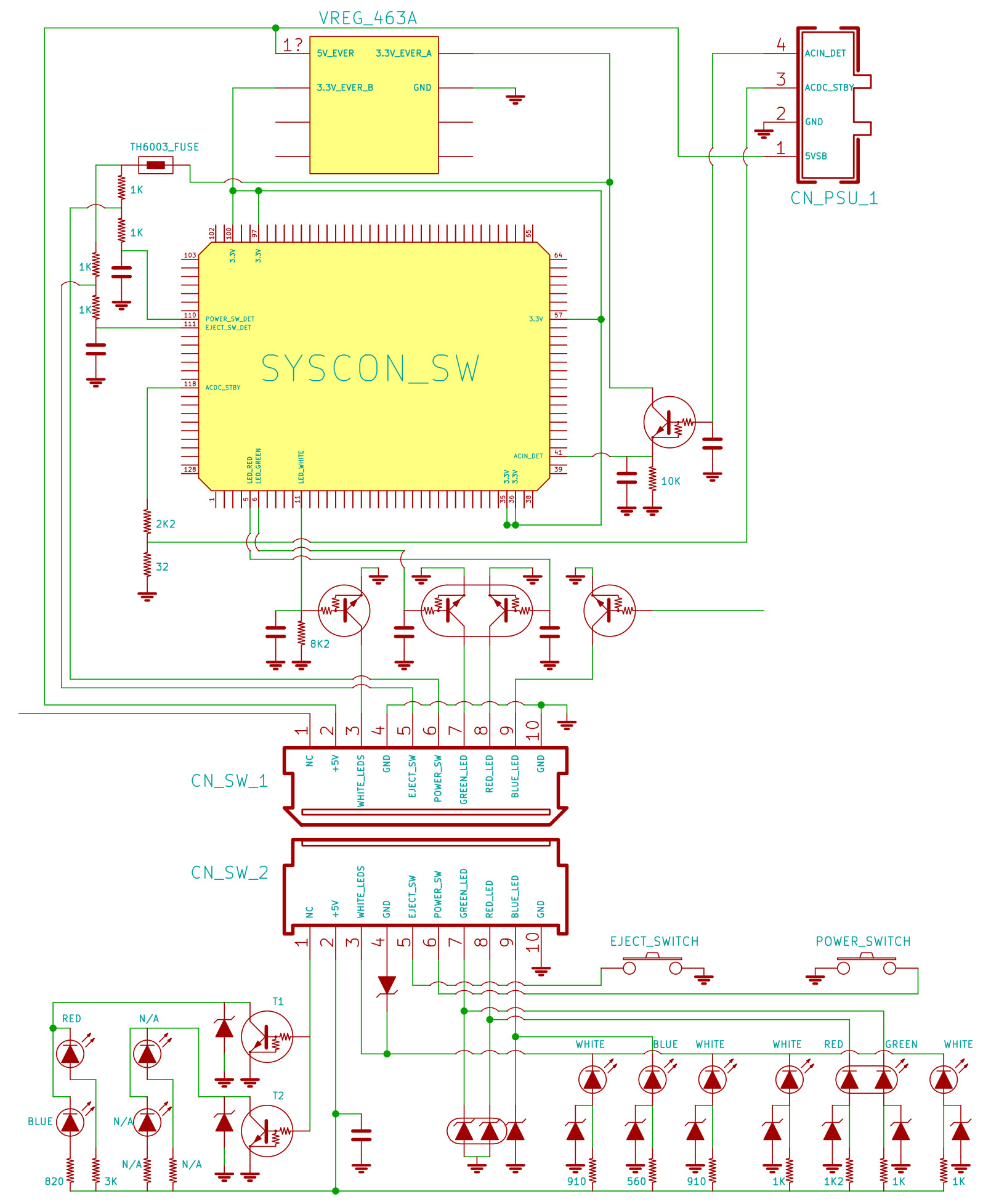
| 3 | 14 | BE_INT/ATTENTION | Connected to CELL pad BA17 through a NPN transistor (CELL switches the transistor to connect this pin to GND) | 3V @ standby (3.15V) | ||
| 4 | 12 | P120/INTP0/EXLVI | Connected to +12V_MAIN through a resistor and divider (EXLVI config = External potential input for low-voltage detector ?) | 0 | ||
| 5 | 3 | P37 | POW_LED | Connected to Switch board dual led (Green) through a dual digital NPN transistor EMH1(SOT-563) | 0 | |
| 6 | 3 | P36 | STBY_LED | Connected to Switch board dual led (Red) through a dual digital NPN transistor EMH1(SOT-563) | 3v @ standby (3.3V) | |
| 7 | 3 | P35 | Connected to South Bridge CXD9963GB pad AA18 | 0 | ||
| 8 | 3 | P34 | Connected to South Bridge CXD9963GB pad AA17 | 0 | ||
| 9 | 3 | P33 | CELL BE related? | 0 | ||
| 10 | 3 | P32 | 0 | |||
| 11 | 16 | BACK_LEDS | Connected to Switch board backlit LEDs through a transistor | 0 | ||
| 12 | 16 | SW_PWM ? | Connected to Switch board contour LEDs through a transistor | 0 | ||
| 13 | 16 | NOT_CONNECTED. Floating through a missing SMD component. See: NOWHERE | 0 | |||
| 14 | 16 | NOT_CONNECTED. Floating through a missing SMD component at the other side of the board. See: VIA | 0 | |||
| 15 | 4 | P47/INTP2 | BT_WAKEON ? | Connected to Wifi/BT module | 0 | |
| 16 | 4 | BUZZER | Connected to the Buzzer through a transistor | 0 | ||
| 17 | 4 | P45/SO01 | Connected to South Bridge CXD9963GB ? (SB_SPI_DO) | 0 | ||
| 18 | 4 | P44/SI01 | Connected to South Bridge CXD9963GB ? (SB_SPI_DI) | 3v @ standby | ||
| 19 | 4 | P43/SCK01 | Connected to South Bridge CXD9963GB ? (SB_SPI_CLK) | 0 | ||
| 20 | 4 | P42/TI04/TO04 | Connected to South Bridge CXD9963GB ? (SB_SPI_CS) | 0 | ||
| 21 | 4 | TOOL_CLK | Connected to Service Connector 3rd Gen. pin 13 (Tool clock) through a missing resistor | 3.0 | ||
| 22 | 4 | TOOL_DAT | Connected to Service Connector 3rd Gen. pin 7 (Tool Data) through a missing resistor | 0 | ||
| 23 | 12 | P127/SO21 | 0 | |||
| 24 | 12 | THR_I2C_SDA | Connected to Temperature Monitors pin 7 (SMBus data) | 3v @ standby (3.15) | ||
| 25 | 12 | THR_I2C_SCL | Connected to Temperature Monitors pin 8 (SMBus clock) | 3v @ standby (3.15) | ||
| 26 | RESET | RESET | Connected to Service Connector 3rd Gen. pin 9 through a missing resistor Connected to standby voltage regulator 463A pin 3 |
|||
| 27 | 12 | XT_SUB/OSCOUT ? | Connected to a crystal (Subsystem clock). CLK -> 1-2V Amplitude (32.768Khz) | |||
| 28 | 12 | XT_SUB/OSCIN ? | Connected to a crystal (Subsystem clock). CLK -> 1-2V Amplitude (32.768Khz) | |||
| 29 | FLMD0 | FLASH_MODE | Connected to Service Connector 3rd Gen. pin 8 (Flash programming mode) through a missing resistor | 3.33 | ||
| 30 | 12 | XT_MAIN/XTAL ? | Connected to a crystal (Main system clock) marked "EX" (16.9344Mhz?) | 0.8v @ standby (1.1) | ||
| 31 | 12 | XT_MAIN/EXTAL ? | Connected to a crystal (Main system clock) marked "EX" (16.9344Mhz?) | 2.2v @ standby (2.4) | ||
| 32 | REGC | VREG_CAP | Connected to battery+ through 2 diodes Connected to a capacitor (internal voltage regulator, around 1uF) at the other side of the board. See: VIA |
|||
| 33 | VSS0 | GND | 0 | |||
| 34 | EVSS0 | GND | 0 | |||
| 35 | VDD | 3.3_EVER_B | Connected to standby voltage regulator 463A pin 2 | 3v @ standby (3.3) | ||
| 36 | EVDD0 | 3.3_EVER_B | Connected to standby voltage regulator 463A pin 2 | 3v @ standby (3.3) | ||
| 37 | 6 | MK_I2C_SCL | Connected to Texas Instruments-SCEI Clock Generator CDC972 pin 37 | 0.2v @ standby | ||
| 38 | 6 | MK_I2C_SDA | Connected to Texas Instruments-SCEI Clock Generator CDC972 pin 38 | 0.2v @ standby | ||
| 39 | 6 | P62 | 0 | |||
| 40 | 6 | P63 | P63_DOWN | 10K resistor to GND | 0 | |
| 41 | 3 | ACIN_DET | Connected to Power Supply control connector pin 4 through a transistor. See: schematic | 3v @ standby (3.3) | ||
| 42 | 6 | P64/RD | Connected to voltage regulator BD9684 0906 pin 4 (enable something) through some undocumented components | 0 | ||
| 43 | 6 | P65/WR0 | Connected to Service Connector 3rd Gen. pin 12 through a missing resistor | 3.0 | ||
| 44 | 6 | P66/WR1 | 0 | |||
| 45 | 6 | NOT_CONNECTED. | 0 | |||
| 46 | 7 | P77/EX23/KR7/INTP11 | Connected to CELL BE through a transistor (labeled 26 and located near the CELL temperature monitor) It seems to be some kind of ALERT signal (inverted direction than the signal from pin 109) |
0 | ||
| 47 | 7 | P76/EX22/KR6/INTP10 | 3v @ standby (3.15) | |||
| 48 | 7 | P75/EX21/KR5/INTP9 | Connected to RSX through a transistor (labeled ND and located near the RSX temperature monitor) It seems to be some kind of ALERT signal |
3v @ standby (3.15) | ||
| 49 | 7 | INTP8_DOWN | 10K resistor to GND | 0 | ||
| 50 | 7 | P73/EX19/KR3 | Connected to Service Connector 3rd Gen. pin 3 Connected to voltage regulator D35653 0S25 (FLASH_ENABLE ?) |
0 | ||
| 51 | 7 | P72/EX18/KR2 | Connected to xxxxxxxxxxxxxx through transistor | 0 | ||
| 52 | 7 | P71/EX17/KR1 | Connected to voltage regulator BD3525 pin 12 (enable something) | 0 | ||
| 53 | 7 | P70/EX16/KR0 | 0 | |||
| 54 | 0 | P06 |
P06_DOWN | 45K resistor array to GND | 0 | |
| 55 | 0 | P05 |
P05_DOWN | 45K resistor array to GND | 0 | |
| 56 | EVSS1 | GND | 0 | |||
| 57 | EVDD1 | 3.3_EVER_B | Connected to standby voltage regulator 463A pin 2 | 3v @ standby (3.3) | ||
| 58 | 8 | P80/EX0 | 0 | |||
| 59 | 8 | P81/EX1 | 0 | |||
| 60 | 8 | P82/EX2 | 0 | |||
| 61 | 8 | P83/EX3 | 0 | |||
| 62 | 8 | P84/EX4 | 0 | |||
| 63 | 8 | P85/EX5 | 0 | |||
| 64 | 8 | P86/EX6 | 0 | |||
| 65 | 8 | P87/EX7 | 0 | |||
| 66 | 3 | P30/INTP3/RTC1HZ | 0 | |||
| 67 | 5 | P50/EX8 | 0 | |||
| 68 | 5 | P51/EX9 | 0 | |||
| 69 | 5 | P52/EX10 | 0 | |||
| 70 | 5 | P53/EX11 | 0 | |||
| 71 | 5 | P54/EX12 | 0 | |||
| 72 | 5 | P55/EX13 | 0 | |||
| 73 | 5 | P56/EX14 | 0 | |||
| 74 | 5 | P57/EX15 | 0 | |||
| 75 | 1 | P17/EX31/TI02/TO02 | Connected to voltage regulator Mitsumi 040 810X pin 5 | 0 | ||
| 76 | 1 | P16/EX30/TI01/TO01/INTP5 | 3v @ standby (3.15) | |||
| 77 | 1 | P15/EX29/RTCDIV/RTCCL | 3v @ standby (3.3) | |||
| 78 | 1 | SC_RxD | Connected to Service Connector 3rd Gen. pin 11 (UART-TTL terminal Receive) through a missing resistor Connected to PCI Connector pin 6 |
0 | ||
| 79 | 1 | SC_TxD | Connected to Service Connector 3rd Gen. pin 10 (UART-TTL terminal Transmit) through a missing resistor Connected to PCI Connector pin 4 |
3.3 | ||
| 80 | 1 | BE_SPI_DI | Connected to CELL pad. (MOSI) Serial Output from Syscon Master to Cell Slave | 0 | ||
| 81 | 1 | BE_SPI_DO | Connected to CELL pad. (MISO) Serial Input from Cell Slave to Syscon Master | 1.2 | ||
| 82 | 1 | BE_SPI_CLK | Connected to CELL pad. 2.5 Mhz SPI Clock | |||
| 83 | 9 | P90/EX32 | /BE_SPI_CS | Connected to CELL pad. Chip Select | 2.0 | |
| 84 | 9 | P91/EX33 | 3v @ standby | |||
| 85 | 9 | P92/EX34 | 0 | |||
| 86 | 9 | P93/EX35 | 0 | |||
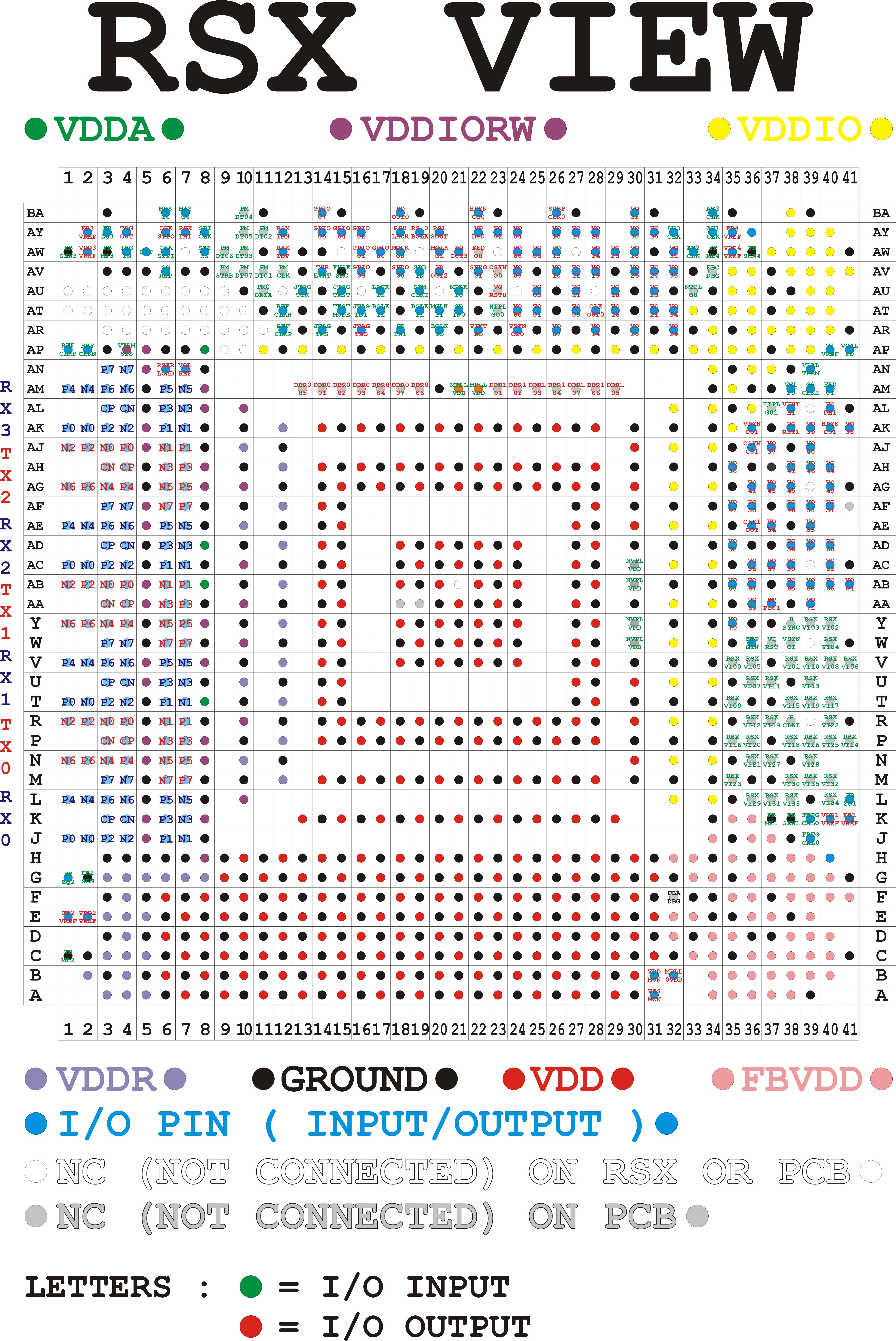
| 87 | 9 | P94 | Connected to RSX pad AW8 ? (RSX_SPI_CS). See: Template:RSX pad layout 41x41 and pad AW8 | 0 | ||
| 88 | 9 | P95/SCK11/SCL11 | Connected to RSX pad AY8 ? (RSX_SPI_CLK ). See: Template:RSX pad layout 41x41 and pad AY8 | 0 | ||
| 89 | 9 | P96/SI11/SDA11 | Connected to RSX pad BA7 ? (RSX_SPI_DI). See: Template:RSX pad layout 41x41 and pad BA7 | 0 | ||
| 90 | 9 | P97/SO11 | Connected to RSX pad BS6 ? (RSX_SPI_DO). See: Template:RSX pad layout 41x41 and pad BA6 | 0 | ||
| 91 | 11 | P112 | 0 | |||
| 92 | 11 | P113 | Connected to voltage regulator BD3527 pin 12 (located near FLASH) | 0 | ||
| 93 | 11 | P114 | 0 | |||
| 94 | 11 | P115 | Connected to xxxxxxxxxxxxxx through transistor | 0 | ||
| 95 | 11 | P116 | Connected to voltage regulator BD3527 pin 12 (located near USB) | 0 | ||
| 96 | 11 | P117 | AV_EN | Connected to MultiAV connector pin 3 (+5V output) through a transistor | 0 | |
| 97 | AVREF1 | 3.3_EVER_B | Connected to standby voltage regulator 463A pin 2 | 3v @ standby (3.3) | ||
| 98 | 11 | NOT_CONNECTED. | 0 | |||
| 99 | 11 | NOT_CONNECTED. | 0 | |||
| 100 | AVREF0 | 3.3_EVER_B | Connected to standby voltage regulator 463A pin 2 | 3v @ standby (3.3) | ||
| 101 | AVSS0 | GND | 0 | |||
| 102 | 15 | ANI15_DOWN | 100k resistor to GND. And to a missing SMD component to VIA to pin 8 of voltage regulator 463A (3.3_EVER_A) | 0 | ||
| 103 | 15 | ANI14_UP | VIA to 100k resistor to pin 8 of voltage regulator 463A (3.3_EVER_A) | 0 | ||
| 104 | 15 | ANI13_DOWN | VIA to 100k resistor to GND | 0 | ||
| 105 | 15 | NOT_CONNECTED. | 0 | |||
| 106 | 15 | NOT_CONNECTED. | 0 | |||
| 107 | 15 | NOT_CONNECTED. | 0 | |||
| 108 | 15 | NOT_CONNECTED. | 0 | |||
| 109 | 15 | ANI8_UP_UNK | Connected to CELL BE through a transistor (labeled ND and located near the CELL temperature monitor) It seems to be some kind of ALERT signal (inverted direction than the signal from pin 46) And to 10k resistor to VIA to pin 8 of voltage regulator 463A (3.3_EVER_A) |
3v @ standby | ||
| 110 | 2 | POW_SW | Connected to Switch board power switch | 3v @ standby (3.3) 3.3 | ||
| 111 | 2 | EJECT_SW | Connected to Switch board eject switch | 3v @ standby (3.3) 3.3 | ||
| 112 | 2 | P25/ANI5 | WIFI_DATA_1 | Connected to Wifi/BT module | 0 | |
| 113 | 2 | P24/ANI4 | WIFI_DATA_2 | Connected to Wifi/BT module | 0 | |
| 114 | 2 | P23/ANI3 | 0 | |||
| 115 | 2 | P22/ANI2 | 0 | |||
| 116 | 2 | P21/ANI1 | 0 | |||
| 117 | 2 | P20/ANI0 | (0V?) | |||
| 118 | 13 | P130 | ACDC_STBY | Connected to Power Supply control connector pin 3 through a 2K2ohm resistor. See: schematic | 3v @ standby (3.3) | |
| 119 | 13 | P131 |
HDMI_EN | Connected to HDMI controller MN8647091 (primary and secondary power inputs) through voltage regulator 348A pins 2 and 7 Connected to HDMI connector pin 18 (+5V output) through a transistor |
3v @ standby (3.3) | |
| 120 | 0 | P07 | 0 | |||
| 121 | 0 | DVE_I2C_SCL | Connected to Digital Video Encoder CXM4027R pin 35 | 0 | ||
| 122 | 0 | DVE_I2C_SDA | Connected to Digital Video Encoder CXM4027R pin 36 | 0 | ||
| 123 | 0 | P02/SO10/TxD1 | 0 | |||
| 124 | 0 | P01/TO00 | Connected to HDMI controller MN8647091 pin 93 | 0 | ||
| 125 | 0 | P00/TI00 | 0 | |||
| 126 | 14 | FANPWM0 | Connected to the FAN grey wire (PWM duty) | 0 | ||
| 127 | 14 | P144/SO20/TxD2 | 0 | |||
| 128 | 14 | HDMI_I2C_SDA ? | Connected to HDMI controller MN8647091 pin 29 | 0 | ||