Media: Difference between revisions
| Line 100: | Line 100: | ||
==== Pinout standard SD (for comparison) ==== | ==== Pinout standard SD (for comparison) ==== | ||
[[File:SD_&_microSD_pins.jpg|280px|thumb|right|SD & microSD pins]] | |||
[[File:SD_card_architecture.jpg|280px|thumb|right|SD card architecture]] | |||
{| class="wikitable" style="text-align: center;border:3px solid #123AAA;" | {| class="wikitable" style="text-align: center;border:3px solid #123AAA;" | ||
| Line 115: | Line 114: | ||
| 2 || CMD || I/O || PP,OD || Command, Response | | 2 || CMD || I/O || PP,OD || Command, Response | ||
|- | |- | ||
| 3 || | | 3 || VSS1 || S || S || Ground | ||
|- | |- | ||
| 4 || | | 4 || VDD || S || S || Power | ||
|- | |- | ||
| 5 || CLK || I || PP || Clock | | 5 || CLK || I || PP || Clock | ||
|- | |- | ||
| 6 || | | 6 || VSS2 || S || S || Ground | ||
|- | |- | ||
| 7 || DAT0 || I/O || PP || Data 0 | | 7 || DAT0 || I/O || PP || Data 0 | ||
| Line 133: | Line 132: | ||
# PP = Push-Pull logic, OD = Open-Drain logic. | # PP = Push-Pull logic, OD = Open-Drain logic. | ||
# S = Power Supply, NC = Not Connected (or logical high). | # S = Power Supply, NC = Not Connected (or logical high). | ||
# The extended DAT lines (DAT1-DAT3) are input on power up. They start to operate as DAT lines after the SET_BUS_WIDTH command. It is the responsibility of the host designer to connect external pullup resistors to all data lines even if only DAT0 is to be used. Otherwise, non-expected high current consumption may occur due to the floating inputs of DAT1 & DAT2 (in case they are not used). | # The extended DAT lines (DAT1-DAT3) are input on power up. They start to operate as DAT lines after the SET_BUS_WIDTH command.<br/> It is the responsibility of the host designer to connect external pullup resistors to all data lines even if only DAT0 is to be used.<br/> Otherwise, non-expected high current consumption may occur due to the floating inputs of DAT1 & DAT2 (in case they are not used). | ||
# After power up, DAT3 is input with 50Kohm(+/-20Kohm) pull-up (can be used for card detection or SPI mode selection | # After power up, DAT3 is input with 50Kohm(+/-20Kohm) pull-up (can be used for card detection or SPI mode selection.<br/> The pull-up may be disconnected by the user, during regular data transfer, with SET_CLR_CARD_DETECT (ACMD42) command. | ||
{| class="wikitable" style="text-align: center;border:3px solid #123AAA;" | |||
|- | |||
! colspan="5"| '''in SPI Mode''' | |||
|- | |||
! Pin № !! Name !! Type !! Description | |||
|- | |||
| 1 || CS || I || Host to card Chip Select signal (Active low) | |||
|- | |||
| 2 || DataIn || I || Host to card data signal | |||
|- | |||
| 3 || VSS1 || S || Ground | |||
|- | |||
| 4 || VDD || S || Power | |||
|- | |||
| 5 || CLK || I || Host to card clock signal | |||
|- | |||
| 6 || VSS2 || S || Ground | |||
|- | |||
| 7 || DATOut || O/PP || Card to host data signal | |||
|- | |||
| 8 || RSV || I || Reserved | |||
|- | |||
| 9 || RSV || I || Reserved | |||
|} | |||
==== Pinout MS & MS M2 (PSP) ==== | ==== Pinout MS & MS M2 (PSP) ==== | ||
Revision as of 14:11, 23 March 2015

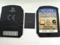
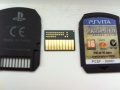
PS Vita Cards
Two types of cards: Gamecards (on which games are sold) and Memorycards (to hold your savedata for games that don't use the storage on the Gamecards)
PS Vita Gamecards


10 pin SD sized card (physical incompatible). ±1.4mm pitch.
Savegames stored on the Gamecards cannot be copied/exported.
Currently produced as 2GB and 4GB cards.
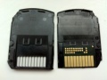
How to disassemble vita game cartridges (and reassemble it)
Pinout
| Pin | Signal | Description |
|---|---|---|
| 1 | VSS | |
| 2 | ||
| 3 | VSS | |
| 4 | ||
| 5 | ||
| 6 | ||
| 7 | ||
| 8 | ||
| 9 | VSS | |
| 10 | VCC | |

Ps-vita - gamecard / memorycard
img1
img3
img6
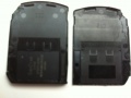
img7
PS Vita Gamecard - inside pic1
PS Vita Gamecard - inside pic2
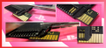
PS Vita Gamecard - inside pic3
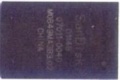
PSVita Gamecard - inside module - topside : 'SanDisk D1149 07011-004G MOB49MA3B3.02 China'
PS Vita Gamecard - dumped content


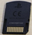
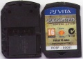
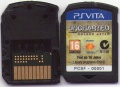
PS Vita Memorycards
PS Vita memory cards come in five variants:
- 4 GB (€ 12 to € 30 -> €3 to 7,5 per GB)
- 8 GB (€ 26 to € 46 -> €3,25 to € 5,75 per GB)
- 16 GB (€ 35 to € 55 -> €2,1875 to € 3,4375 per GB)
- 32 GB (€ 65,- -> € 2,03125 per GB)
- 64 GB (9580 yen, ~$94 -> $1,46875 per GB)
note: current sales price as listed in Pricewatch

Pinout
don't try to take it apart like this
| Pin | Signal | Description |
|---|---|---|
| 1 | ||
| 2 | ||
| 3 | ||
| 4 | ||
| 5 | ||
| 6 | ||
| 7 | ||
| 8 | ||
| 9 |
Pinout standard SD (for comparison)


| in SD Card Mode | ||||
|---|---|---|---|---|
| Pin № | Name | I/O | Logic | Description |
| 1 | DAT3 | I/O | PP | Data 3 |
| 2 | CMD | I/O | PP,OD | Command, Response |
| 3 | VSS1 | S | S | Ground |
| 4 | VDD | S | S | Power |
| 5 | CLK | I | PP | Clock |
| 6 | VSS2 | S | S | Ground |
| 7 | DAT0 | I/O | PP | Data 0 |
| 8 | DAT1 nIRQ |
I/O O |
PP OD |
Data 1. SDIO Cards share with Interrupt Period |
| 9 | DAT2 | I/O | PP | Data 2 |
Notes:
- Direction is relative to card. I = Input, O = Output.
- PP = Push-Pull logic, OD = Open-Drain logic.
- S = Power Supply, NC = Not Connected (or logical high).
- The extended DAT lines (DAT1-DAT3) are input on power up. They start to operate as DAT lines after the SET_BUS_WIDTH command.
It is the responsibility of the host designer to connect external pullup resistors to all data lines even if only DAT0 is to be used.
Otherwise, non-expected high current consumption may occur due to the floating inputs of DAT1 & DAT2 (in case they are not used). - After power up, DAT3 is input with 50Kohm(+/-20Kohm) pull-up (can be used for card detection or SPI mode selection.
The pull-up may be disconnected by the user, during regular data transfer, with SET_CLR_CARD_DETECT (ACMD42) command.
| in SPI Mode | ||||
|---|---|---|---|---|
| Pin № | Name | Type | Description | |
| 1 | CS | I | Host to card Chip Select signal (Active low) | |
| 2 | DataIn | I | Host to card data signal | |
| 3 | VSS1 | S | Ground | |
| 4 | VDD | S | Power | |
| 5 | CLK | I | Host to card clock signal | |
| 6 | VSS2 | S | Ground | |
| 7 | DATOut | O/PP | Card to host data signal | |
| 8 | RSV | I | Reserved | |
| 9 | RSV | I | Reserved | |