CXR713120-201GB: Difference between revisions
Jump to navigation
Jump to search
m (Photos moved to CXR714120-301GB) |
m (Moved to Syscon Hardware) |
||
| Line 1: | Line 1: | ||
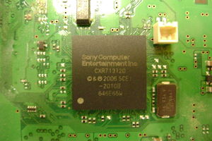
== | == Syscon CXR713120-201GB == | ||
<div style="float:right">[[File:SYSCON_GEN1.JPG|thumb|Syscon [[CXR713120-201GB]]]]</div> | <div style="float:right">[[File:SYSCON_GEN1.JPG|thumb|Syscon [[CXR713120-201GB]]]]</div> | ||
*Used in PS3 models: | |||
**[[CECHAxx]] and [[CECHBxx]] with [[COK-001]] motherboard | |||
8-753-279-04 / IC4002 | |||
<br style="clear: both;" /> | <br style="clear: both;" /> | ||
=== Pinout === | === Pinout === | ||
{{Syscon Pinout BGA 200 pads}} | {{Syscon Pinout BGA 200 pads}} | ||
{{Motherboard Components}}<noinclude>[[Category:Main]]</noinclude> | {{Motherboard Components}}<noinclude>[[Category:Main]]</noinclude> | ||
Revision as of 21:11, 29 May 2021
Syscon CXR713120-201GB

Syscon CXR713120-201GB
8-753-279-04 / IC4002
Pinout
Template:Syscon Pinout BGA 200 pads
| |||||||||||||||||||||||||||||||||||||||||||||||||||||||||||||||||||||||||||||||||||||||||||||||||||||||||||||||||||||||||||||||||||||||||||||||||||||||||||||||||||||||||||||
