CXR713120-201GB
Jump to navigation
Jump to search
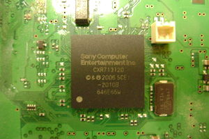
Generation 1: CXR713120-201GB / CXR713120-201GB-TL (SysCon)

Syscon CXR713120-201GB
8-753-279-04 / IC4002
Early PS3 : up to including CECHKxx/DIA-002
Pinout
Template:Syscon Pinout BGA 200 pads
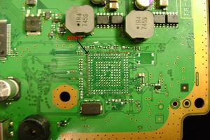
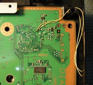
Intercepting signals
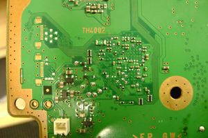
This points are availables to intercept signals by soldering wires, attaching probes, osciloscopes, etc... The photos are only orientatives to follow the traces, there's no need to remove the SYSCON to intercept this signals so can be done while its working
All this points has been hardware reverse engineered from a CECHH02/DIA-001 motherboard
Topside Pinout
| Pin # | Name | Description |
|---|---|---|
| B3 | SW_10 | Unknown |
| A6 | MC_RESERVED2 | Unknown |
| E10 | MUL_CHKSTP_OUT | Unknown |
| C15 | VSS | Power Ground |
| B16 | OSCOUT | Goes to unpopulated crystal |
| C16 | OSCIN | From unpupulated crystal |
| B15 | POW_FAIL | Power Failure Signal |
| H1 | PN5 | Unknown |
| H2 | PN6 | Unknown |
| R1 | PM7 | Unknown |
| R2 | PM6 | Unknown |
| M4 | SW9 | Unknown |
| M10 | XDR_FET_SCK | Unknown |
Bottomside Pinout
| Pin # | Name | Description |
|---|---|---|
| R5 | VDD | +3.3v |
| R7 | DVDD | +1.8v |
| C15 | VSS | Power Ground |
| N16 | DIAG_MODE | Unknown |
| N15 | BACKUP_MODE | Unknown |
| P16 | UART0_TxD | Serial |
| P15 | UART0_RxD | Serial |
| R9 | PQ1 | Unknown |
| B12 | POW_SW | Power Switch |
| A12 | EJECT_SW | Eject Switch |
| L7 | JNTAST | JTAG |
| L8 | JRTCK | JTAG |
| L9 | JTMS | JTAG |
| K7 | JTDI | JTAG |
| K8 | JTCK | JTAG |
| K9 | JTDO | JTAG |
| M6 | SW_7_B | Unknown |
| M8 | FANPWM1 | Unknown |
| E5 | GX_VSRT | Unknown |
| B5 | DVE_RST | Unknown |
| G4 | HDMI_RST1 | Unknown |
| D4 | XDR_FET_RST | Unknown |
| |||||||||||||||||||||||||||||||||||||||||||||||||||||||||||||||||||||||||||||||||||||||||||||||||||||||||||||||||||||||||||||||||||||||||||||||||||||||||||||||||||||||||||||


