Talk:Switch boards: Difference between revisions
m (old speculation removed, only one sentence was right... the misterious pin goes to syscon hidden in internal layers of the motherboard and probably all them shielded in between ground layers) |
|||
| (10 intermediate revisions by 2 users not shown) | |||
| Line 1: | Line 1: | ||
== Pin 1 identification == | |||
All components whose pins needs to be marked in electronic equipment (because the component has several pins, like any chip/IC or connectors) always has a mark in pin 1... sometimes this mark is not visible because is "printed" under the component itself (so only visible before soldering the component to the board)... this seems to be the case in some of the connectors in PS3 power/eject boards, so the identification of pin 1 can be confusing | |||
As example... HSW-001 board has a "copper point" marked close to the connector... but this point is the ground pin of the capacitor placed below (the blue text in the first photo is wrong because this point is not related with the connector). So there is no way to identify pin1 by looking at HSW-001 board... the solution is to look at the connector in the other side of the ribbon cable (in other words... in the main motherboard) | |||
The | <gallery> | ||
File:Power Eject board HSW-001 (Connector pin 1 detail).jpg|The blue text is wrong because this point is not related with the connector but this is actually pin 1 if you look at the motherboard and trace it along the ribbon cable | |||
File:Power Eject board HSW-001 (JSD-001) schematic.jpg|But by looking at this photo of the motherboard is visible another point that is actually the pin 1 mark of the connector | |||
</gallery> | |||
==Non retail Switch boards== | |||
[[SW-13]], used in [[COOKIE-13]] | |||
<gallery> | |||
File:COKIE-13-33.jpg|COOKIE-13 ([[CSW-001]] [[SW-13]]_B) | |||
File:COKIE-13-32.jpg|COOKIE-13 ([[CSW-001]] [[SW-13]]_A) | |||
</gallery> | |||
Latest revision as of 04:39, 19 July 2017
Pin 1 identification[edit source]
All components whose pins needs to be marked in electronic equipment (because the component has several pins, like any chip/IC or connectors) always has a mark in pin 1... sometimes this mark is not visible because is "printed" under the component itself (so only visible before soldering the component to the board)... this seems to be the case in some of the connectors in PS3 power/eject boards, so the identification of pin 1 can be confusing
As example... HSW-001 board has a "copper point" marked close to the connector... but this point is the ground pin of the capacitor placed below (the blue text in the first photo is wrong because this point is not related with the connector). So there is no way to identify pin1 by looking at HSW-001 board... the solution is to look at the connector in the other side of the ribbon cable (in other words... in the main motherboard)
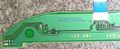
The blue text is wrong because this point is not related with the connector but this is actually pin 1 if you look at the motherboard and trace it along the ribbon cable
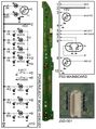
But by looking at this photo of the motherboard is visible another point that is actually the pin 1 mark of the connector
_schematic.jpg)
