Ernie: Difference between revisions
Jump to navigation
Jump to search
m (Text replacement - "<imgur(?:\s+\w+=(?:\w+|"[^"]+"))*\s*>([^<]+?\.(jpg|jpeg|png|gif))\s*<\/imgur>" to "200px") |
|||
| (49 intermediate revisions by 6 users not shown) | |||
| Line 1: | Line 1: | ||
Ernie is the codename for PSVita Syscon. | |||
= Talking to Ernie = | = Pictures = | ||
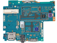
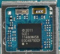
* [[File:xzonnpr.png|200px]](source ifixit, denoted id 1148KM458) | |||
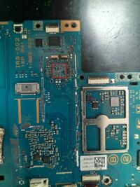
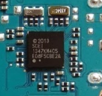
* [[File:Pmsm2bJ.jpg|200px]](denoted red) | |||
* [[File:fVyL18x.jpg|200px]] | |||
* [[File:AS3Dzti.png|200px]] | |||
* [[File:BN2JA8g.png|200px]] | |||
* [[File:7avGDL7.png|200px]] | |||
* [[File:eYTpTOI.png|200px]] | |||
* [[File:hwzb7TN.png|200px]] | |||
* [[File:hwCbt3f.png|200px]] | |||
SCEI 1148KM458: | |||
[[File:SCEI 1148KM458 mit20x dirty small.png]] | |||
= Talking to Ernie (RL78) = | |||
<pre> | <pre> | ||
| Line 20: | Line 35: | ||
</pre> | </pre> | ||
= Some pics (testpoints, layout, blank vs not blank) = | = Talking to Ernie (78K0R) = | ||
<pre> | |||
02 1b 10 ef 04 dc fd fd ff ff 03 44 37 39 46 30 31 30 39 20 20 f8 03 00 00 00 ff ff ff 0f 03 | |||
</pre> | |||
<pre> | |||
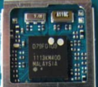
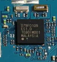
Device: D79F0109 | |||
</pre> | |||
<pre> | |||
STX: 0x02 | |||
LEN: 0x1B | |||
Vendor Code: NEC (0x10) | |||
Macro Extension Code: 0xEF | |||
Macro Function Code: 0x04 | |||
Device Extension Codes 1 and 2: 0xDC FD | |||
User Flash Rom Last Adress: ff ff 03 (0x40000) | |||
Device Name (10 bytes) 44 37 39 46 30 31 30 39 20 20 (D79F0109 ) | |||
Security Flag: 0xF8 | |||
Boot Block Number: 0x03 | |||
Start Block: 00 00 | |||
End Block : 00 ff | |||
Reserved: FF FF | |||
Checksum: 0x0F | |||
ETX: 0x03 | |||
</pre> | |||
= How to talk = | |||
{| class="wikitable" | |||
|- | |||
! E1/E20/E2 Emulator, E2 Emulator Lite !! Syscon !! Notes | |||
|- | |||
| TOOL0 || TOOL0 || Pull up the signals of the TOOL0 pin at 1 kΩ and do not arrange these signal lines in parallel with or | |||
across other high-speed signal lines. | |||
|- | |||
| RESET || RESET || When flash programming by the programming software is to be performed, the RESET# pin should be designed so that the reset signal on the user system does not conflict with the reset signal from the E1/E20/E2/E2 Lite. | |||
|- | |||
| GND || GND || The pins of the connector marked "GND" must be at the same ground level as the VSS pin of the MCU. | |||
|- | |||
| VDD || VDD || Connect the VDD of the connector to the VDD (power supply) of the user system. Use the emulator within the power supply voltage of 1.8 V to 5.5 V and within the operating voltage range of the MCU. | |||
|- | |||
| EVDD || EVDD || | |||
|} | |||
= Identifying VDD/EVDD = | |||
<pre> | |||
killing evdd kills Tool0 but not I2C, but vdd kills both | |||
2.5V is vdd, 1.8V is evdd0/1 | |||
evdd voltage is used for reset for some weird reason | |||
</pre> | |||
= Some RL78 pics (testpoints, layout, blank vs not blank, options) = | |||
[[File:e9FGck8.png|200px]] | |||
[[File:nq4LID7.png|200px]] | |||
[[File:6ASfhB1.png|200px]] | |||
[[File:yAWXJnK.png|200px]] | |||
[[File:kKhSCdm.png|200px]] | |||
= Some 78K0R pics = | |||
* [[File:FEBXKkk.png|200px]] | |||
* [[File:jZgJNwF.png|200px]] | |||
== Pinout == | |||
* VDD, TOOL0 and RESET known | |||
* TOOL1, FLMD0 and GND Unknown | |||
* F9, F5, F6, J3, J10, G10, F10, H1, H4 possible | |||
* F9, F10, G10, J10, most likely candidates respectively to TOOL0 TOOL1 RESET FLMD0 | |||
* F6 is VDD, F9 TOOL0, G10 RESET | |||
= Debugger Points for Glitching = | = Debugger Points for Glitching = | ||
<pre> | <pre> | ||
J1 EVDD | |||
C10, F6(Optional) VDD | |||
F11 GND | |||
F9 TOOL0 | F9 TOOL0 | ||
G10 FLMD0 (On Old 78K0R pstv/psvita 1000 boards) | |||
F10 RESET | |||
</pre> | |||
== Glitch Victim Versions == | |||
<pre> | |||
Ernie version: 0x1030505 | |||
Ernie version: 0x1030511 | |||
Unknown version: 3.30 | |||
RL78 Version: 0x0303 | |||
</pre> | </pre> | ||
Latest revision as of 05:16, 4 May 2023
Ernie is the codename for PSVita Syscon.
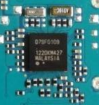
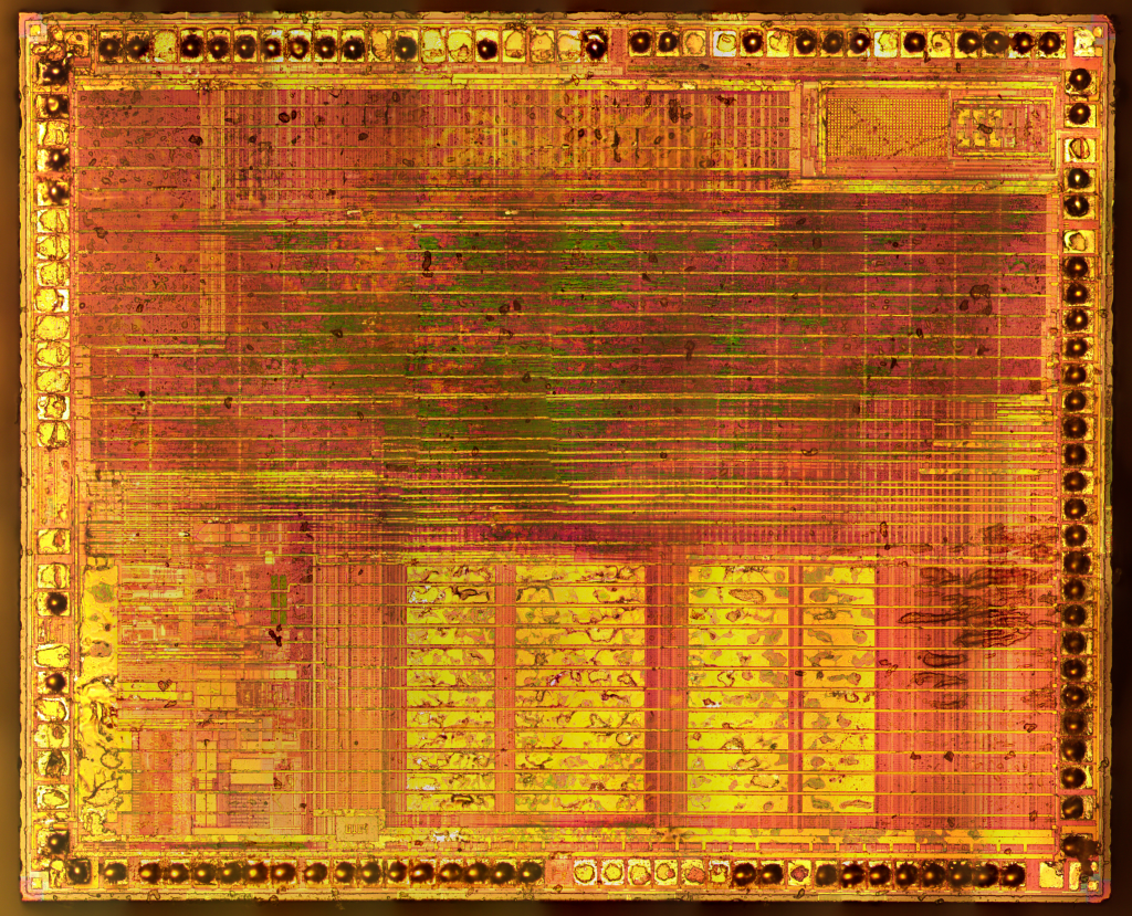
Pictures[edit | edit source]
Talking to Ernie (RL78)[edit | edit source]
Connecting the tool
Tool : E2 Lite, Tool Num : 5ES000599, Interface : 1 wire UART
Emulator's supply power : OFF
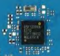
Emulator's firmware version:3.00.00.007
Connecting to the target device
Query the device information.
Device Name : R5F1ZCRK
Devcie Code : 10 00 06
Firmware Version : V3.03
Code Flash 1 (Address : 0x00000000,  Size : 384 K,  Erase Size : 1 K)
Data Flash 1 (Address : 0x000F1000,  Size : 8 K,  Erase Size : 1 K)

Disconnecting the tool
Operation completed.
Talking to Ernie (78K0R)[edit | edit source]
02 1b 10 ef 04 dc fd fd ff ff 03 44 37 39 46 30 31 30 39 20 20 f8 03 00 00 00 ff ff ff 0f 03
Device: D79F0109
STX: 0x02
LEN: 0x1B
Vendor Code: NEC (0x10)
Macro Extension Code: 0xEF
Macro Function Code: 0x04
Device Extension Codes 1 and 2: 0xDC FD
User Flash Rom Last Adress: ff ff 03 (0x40000)
Device Name (10 bytes) 44 37 39 46 30 31 30 39 20 20 (D79F0109  )
Security Flag: 0xF8
Boot Block Number: 0x03
Start Block: 00 00
End Block : 00 ff
Reserved: FF FF
Checksum: 0x0F
ETX: 0x03
How to talk[edit | edit source]
| E1/E20/E2 Emulator, E2 Emulator Lite | Syscon | Notes |
|---|---|---|
| TOOL0 | TOOL0 | Pull up the signals of the TOOL0 pin at 1 kΩ and do not arrange these signal lines in parallel with or
across other high-speed signal lines. |
| RESET | RESET | When flash programming by the programming software is to be performed, the RESET# pin should be designed so that the reset signal on the user system does not conflict with the reset signal from the E1/E20/E2/E2 Lite. |
| GND | GND | The pins of the connector marked "GND" must be at the same ground level as the VSS pin of the MCU. |
| VDD | VDD | Connect the VDD of the connector to the VDD (power supply) of the user system. Use the emulator within the power supply voltage of 1.8 V to 5.5 V and within the operating voltage range of the MCU. |
| EVDD | EVDD |
Identifying VDD/EVDD[edit | edit source]
killing evdd kills Tool0 but not I2C, but vdd kills both
2.5V is vdd, 1.8V is evdd0/1
evdd voltage is used for reset for some weird reason
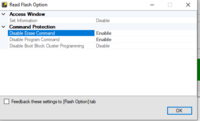
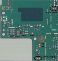
Some RL78 pics (testpoints, layout, blank vs not blank, options)[edit | edit source]
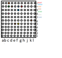
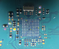
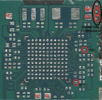
Some 78K0R pics[edit | edit source]
Pinout[edit | edit source]
- VDD, TOOL0 and RESET known
- TOOL1, FLMD0 and GND Unknown
- F9, F5, F6, J3, J10, G10, F10, H1, H4 possible
- F9, F10, G10, J10, most likely candidates respectively to TOOL0 TOOL1 RESET FLMD0
- F6 is VDD, F9 TOOL0, G10 RESET
Debugger Points for Glitching[edit | edit source]
J1     EVDD
C10, F6(Optional)  VDD
F11    GND
F9     TOOL0
G10    FLMD0 (On Old 78K0R pstv/psvita 1000 boards)
F10    RESET
Glitch Victim Versions[edit | edit source]
Ernie version: 0x1030505
Ernie version: 0x1030511
Unknown version: 3.30
RL78 Version: 0x0303
