Validating flash dumps
Why so important?
Whenever you want to mess with flash (NAND or NOR), you have to make sure you are getting 100% correct, valid, verified dumps.
So what can we use to prevent that, and make sure our dumps are as proper as we can check?
Visual inspection
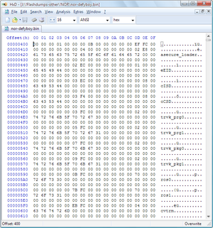
Open up the flashdump (make it unified first if it is still 2 seperate NAND dumps) with a hexeditor (e.g. HxD)
and compare what you see with the Flash page.
Statistical analysis
One neat option in HxD is the analysis option. Open dump file and select Statistics in the Analysis menu. Mouse over the blue graph bars of 00 and FF
Valid dumps will have
| Value | NAND | NOR |
|---|---|---|
| 00's | 1.43% - 2.68% | 18.71% - 29.01% |
| FF's | 18.25% - 24.54% | 10.42% - 10.48% |
| rest | below 0.5% | below 0.5% |
Bytereversed
  00 00 00 00 AC 0F FF E0 00 00 00 00 AD DE EF BE  (HEX)   and   saceru_eoldare  (Text)
  instead of
  00 00 00 00 0F AC E0 FF 00 00 00 00 DE AD BE EF  (HEX)   and   asecure_loader  (Text)
You can use either the bytereverse option in the the flasher application and redump, or bytereverse the current dump with Flowrebuilder.
Only zeroes
00 00 00 00 00 00 00 00 00 where data should've been
- Seems reading is a problem, mostly caused by bad wiring/clip seating -> check
patterned non zeroes / patterned non ff's
  30 30 30 30 30 30 30 30 30 30 30 30 30 30 30 30
  00 80 00 80 00 80 00 80 00 80 00 80 00 80 00 80   where zeroes should've been
EF FF EF FF EF FF EF FF EF FF EF FF EF FF EF FF where FF's should've been
- Seems reading is a problem, mostly caused by bad wiring/clip seating -> check
- Can also be caused by bad grounding, too low Vcc, interference or too long wires -> check
patterned FF's
FF FF FF FF FF FF FF FF FF FF FF FF FF FF FF FF repetive banding of FF's where data or zeroes should have been
- Seems reading is a problem, mostly caused by bad wiring/clip seating -> check
malformed headers / filenames / regionnames
  IJI              instead of   IFI
  asecure_loaher                asecure_loader
  eIIH                          eEID
  cESH                          cISD
  cCSH                          cCSD
  trvg_prk0                     trvk_prg0
  trvg_prk1                     trvk_prg1
  trvg_pkk0                     trvk_pkg0
  trvg_pkk1                     trvk_pkg1
  cztrm                         cvtrm
  mitldr                        metldr
- Seems reading is a problem, mostly caused by bad wiring/clip seating -> check
absent files / regions
00FC0000 FF FF FF FF FF FF FF FF FF FF FF FF FF FF FF FF ÿÿÿÿÿÿÿÿÿÿÿÿÿÿÿÿ missing bootldr in NOR
00000000 FF FF FF FF FF FF FF FF FF FF FF FF FF FF FF FF ÿÿÿÿÿÿÿÿÿÿÿÿÿÿÿÿ missing bootldr in NAND
- Seems reading is a problem, mostly caused by bad wiring/clip seating -> check
malformed files / regions
00FC0000 28 B4 4F D2 F9 3F BC 43 28 B4 4F D2 F9 3F BC 43 (´OÒù?¼C(´OÒù?¼C corrupted bootldr in NOR (it should always start with 00 00 there)
- Seems reading is a problem, mostly caused by bad wiring/clip seating -> check
Repetitions
take 16 bytes of an offset that should be unique, e.g. the 0x10 offset which normaly has the DEADBEEF magic header :
NOR: 0x0000010 00 00 00 00 0F AC E0 FF 00 00 00 00 DE AD BE EF // NAND: 0x040010 00 00 00 00 0F AC E0 FF 00 00 00 00 DE AD BE EF
And find all instances in hexeditor
When it says found in 0x10 and 0x10010 you substract them (0x10010 - 0x10 = 0x10000)
So that means there is an error with setting 0x10000 (only one bit set!) low
because the programmer applies 0x10010 but the actual data on the address lines (received by the nor flash) is 0x10
Checking again with other unique 16 byte sequence
617365637572655F6C6F616465720000 (asecure_loader in hex)
Same check, found at 0x420 and 0x10420 (0x10420-0x420 = 0x10000)
OK, you've found the pattern, now how do we deduct from that the faulty line?
address is 2 bytes. 0x10 in dump with hexeditor is in reality 0x8 on the address bus because we read 2 bytes at once
so the address is no longer 0x10000 but 0x8000
0x8000 (hexadecimal = base 16) = 1000 0000 0000 0000 (binary = base 2)
which means the 16th bit = 1, we start counting at A0, so the 16th is A15
conclusion : A15 is bad
Quick lookup table
| repetition | addressline 'stuck' |
|---|---|
| 0x2 | A0 |
| 0x4 | A1 |
| 0x8 | A2 |
| 0x10 | A3 |
| 0x20 | A4 |
| 0x40 | A5 |
| 0x80 | A6 |
| 0x100 | A7 |
| 0x200 | A8 |
| 0x400 | A9 |
| 0x800 | A10 |
| 0x1000 | A11 |
| 0x2000 | A12 |
| 0x4000 | A13 |
| 0x8000 | A14 |
| 0x10000 | A15 |
| 0x20000 | A16 |
| 0x40000 | A17 |
| 0x80000 | A18 |
| 0x100000 | A19 |
| 0x200000 | A20 |
| 0x400000 | A21 |
| 0x800000 | A22 |
| 0x1000000 | A23 |
| 0x2000000 | A24 |
| 0x4000000 | A25 |
| 0x8000000 | A26 |
| 0x10000000 | A27 |
| 0x20000000 | A28 |
| 0x40000000 | A29 |
| 0x80000000 | A30 |
Check metldr+bootldr sizes
You can check metldr and bootldr sizes easily with HxD
- either after extracting flash with Flowrebuilder and opening seperate files
- or by looking in the unextracted Flash dump at the correct offset.
This table lists some common known values for your convenience as quick lookup:
| IDPS/Product Code | SKU - Datecode / Manufacturing date | metldr offset | bootldr | Notes | lowest known firmware | |||
|---|---|---|---|---|---|---|---|---|
| 0x2F077 (NOR) 0x80877 (NAND) |
0x81E (NOR) 0x4081E (NAND) |
0x842 (NOR) 0x40842 (NAND) |
size | 0xFC0002 (NOR) 0x02 (NAND) |
0xFC0012 (NOR) 0x12 (NAND) | |||
| n/a | CEB-2030 (MPU-501) PROTO | n/a | n/a | 28C20 | 28 BE | 28 BE | Patch + FSM = OK | <=0.50.003 |
| 01 | DEH-Z1010 (TMU-520) SD | 14 20 | 11 3E | 2D020 | 2C FE | 2C FE | Patch + FSM = OK | <=0.80.004 |
| 01 | DECR-1000 (TMU-520) DECR Every DECR manufactured before January 2009 Share the same BL/Metldr revisions | EC 40 | 0E C0 | 2A840 | 2A 80 | 2A 80 | Patch + FSM = OK | <=0.85.010 |
| 01 | ?DEH-H1001-D? (COOKIE13) CEX | EC 40 | 0E C0 | 2A830 | 2A 7F | 2A 7F | Patch + FSM = OK | <=0.85.010 |
| 01 | DEH-H1000A-E (COK-001) DEX | EC 70 | 0E C3 | 2A1E0 | 2A 1A | 2A 1A | Patch + FSM = OK | <095.001 |
| 01 04 |
CECHAxx (COK-001) CECHExx (COK-002) |
EE 10 | 0E DD | 2A430 | 2A 3F | 2A 3F | Patch + FSM = OK | 1.00 1.00 |
| 01 02 03 01 |
CECHAxx (COK-001) with 1.00 from factory CECHBxx (COK-001) CECHCxx (COK-002) DECHAxx (COK-001) DEX |
ED A0 | 0E D6 | 2A2E0 | 2A 2A | 2A 2A | Patch + FSM = OK | 1.00 1.00 1.00 1.00 |
| 03 | CECHCxx (COK-002) with 1.00 from factory | EB F0 | 0E BB | 30480 | 30 44 | 30 44 | Patch + FSM = OK | 1.00 1.00 |
| 01 02 03 |
CECHAxx (COK-001) CECHBxx (COK-001) CECHCxx (COK-002) |
ED E0 | 0E DA | 2A3B0 | 2A 37 | 2A 37 | Patch + FSM = OK | 1.00 1.00 1.00 |
| 04 05 |
Namco System 357 (COK-002) ARC CECHGxx (SEM-001) |
E7 B0 | 0E 77 | 2E900 | 2E 8C | 2E 8C | Patch + FSM = OK | ?1.90? 1.90 |
| 05 06 |
CECHGxx (SEM-001) CECHHxx (DIA-001) |
E7 B0 | 0E 77 | 2F200 | 2F 1C | 2F 1C | Patch + FSM = OK | 2.30 2.30 |
| 05 06 |
CECHGxx (SEM-001) CECHHxx (DIA-001) |
E8 C0 | 0E 88 | 2EF80 | 2E F4 | 2E F4 | Patch + FSM = OK | 2.30 2.30 |
| 06 07 |
CECHHxx (DIA-001) CECHJxx (DIA-002) with 2.30 from factory - datecode 8B |
E8 E0 | 0E 8A | 2EF80 | 2E F4 | 2E F4 | Patch + FSM = OK | 1.97 2.30 |
| 03 06 06 |
CECHExx (COK-002) CECHHxx (DIA-001) CECHMxx (DIA-001) |
EA 60 | 0E A2 | 2EE70 | 2E E3 | 2E E3 | Patch + FSM = OK | 1.97 1.97 |
| 07 | CECHJxx (DIA-002) CECHKxx (DIA-002) datecode 8C |
EA 60 | 0E A2 | 2EE70 | 2E E3 | 2E E3 | Patch + FSM = OK | 2.30 |
| 08 07 08 |
Namco System 357 (VER-001) ARC DECHJxx (DIA-002) DEX CECHLxx / CECHPxx (VER-001) |
E8 D0 | 0E 89 | 2EAF0 | 2E AB | 2E AB | Patch + FSM = OK | ?2.45? 2.16 2.45 |
| 08 | CECHLxx (VER-001) | E8 D0 | 0E 89 | 2EB70 | 2E B3 | 2E B3 | Patch + FSM = OK | 2.45 |
| 08 09 |
CECHLxx (VER-001) with 2.30 from factory - datecode unknown CECH-20xx (DYN-001) with 2.76 from factory, datecode unknown |
E8 90 | 0E 85 | 2F170 | 2F 13 | 2F 13 | Patch + FSM = OK | 2.30 2.70 |
| 09 | DECR-1400 (DEB-001) DECR with 2.60 from factory - manufacture date June 09 |
E8 90 | 0E 85 | 2F170 | 2F 13 | 2F 13 | Patch + FSM = OK | 2.60 |
| 09 | CECH-20xx (DYN-001) | E9 20 | 0E 8E | 2F3F0 | 2F 3B | 2F 3B | Patch + FSM = OK | 2.70 |
| 0A | CECH-21xx (SUR-001) | E9 20 | 0E 8E | 2F4F0 | 2F 4B | 2F 4B | Patch + FSM = OK | 3.20 |
| 03 0B 0B |
CECHExx (COK-002W) refurbished CECH-25xx (JTP-001) with 3.40 from factory - datecode 0C CECH-25xx (JSD-001) with 3.41 from factory - datecode 0C |
E9 20 | 0E 8E | 2F4F0 | 2F 4B | 2F 4B | Patch + FSM = OK | 3.40 3.40 3.40 |
| 0B 0B |
CECH-25xx (JSD-001) with 3.56 from factory - datecode 0D CECH-25xx (JTP-001) with 3.56 from factory - datecode 1A |
E9 60 | 0E 92 | 2F570 | 2F 53 | 2F 53 | Patch + FSM = OK | 3.50 3.50 |
| 0B 0B 0B |
CECH-25xx (JTP-001) with 3.56 from factory - datecode 1A (rare) CECH-25xx (JSD-001) with 3.56 from factory - datecode 1B (common) CECH-25xx (JTP-001) with 3.56 from factory - datecode 1B (common) |
E9 60 | 0E 92 | 2F5F0 | 2F 5B | 2F 5B | (RLOD+)poweroff @ downgrade 355 (3.56+ + spkg fix + signed 3.55 priv : should work) Patch + noFSM = OK |
3.56 3.56 3.56 |
| 0B 0B 0C |
CECH-25xx (JSD-001) with 3.60 from factory - datecode 1B CECH-25xx (JTP-001) with 3.60 from factory - datecode [N.A.] CECH-30xx (KTE-001) with 3.65 from factory - datecode [N.A.] |
F9 20 | 0F 8E | 2FFF0 | 2F FB | 2F FB | "metldr.2" (RLOD+)poweroff @ downgrade 3.55 (RLOD+)poweroff @ Patch + noFSM |
3.60 3.60 3.60 |
| 0C | CECH-30xx (KTE-001) with ? from factory - datecode [?] | F9 B0 | 0F 97 | 30070 | 30 03 | 30 03 | "metldr.2" (RLOD+)poweroff @ downgrade 3.55 (RLOD+)poweroff @ Patch + noFSM |
? |
| 0C | CECH-30xx (KTE-001) with 3.72 from factory - datecode [1C] | F9 B0 | 0F 97 | 300F0 | 30 0B | 30 0B | "metldr.2" (RLOD+)poweroff @ downgrade 3.55 (RLOD+)poweroff @ Patch + noFSM |
3.72 |
| 0D 0D 2C |
CECH-40xx (MSX-001) CECH-40xx (MPX-001) CECH-40xx (MSX-001) '12GB' |
F9 B0 | 0F 97 | 301F0 | 30 1B | 30 1B | "metldr.2" (RLOD+)poweroff @ downgrade 3.55 (RLOD+)poweroff @ Patch + noFSM |
4.20 ? 4.22 |
| 12 | CECH-42xx (PQX-001) '12GB' | F9 B0 | 0F 97 | 301F0 | 30 1B | 30 1B | "metldr.2" (RLOD+)poweroff @ downgrade 3.55 (RLOD+)poweroff @ Patch + noFSM |
4.20 ? 4.22 |
Flowrebuilder
Links to versions
http://www.ps3devwiki.com/files/flash/Tools/Flowrebuilder/
- FlowRebuilder v.4.2.2.0.exe (389 KB) // mirror
- FlowRebuilder v.4.2.1.2.exe (313.50 KB) // mirror
- FlowRebuilder v.4.2.1.1.exe (473.57 KB) // mirror
- FlowRebuilder v.4.2.0.1.exe (474.01 KB) // mirror
- FlowRebuilder v.4.1.3.2.exe (459.95 KB) // mirror
- FlowRebuilder v.4.1.0.0.exe (454.85 KB) // mirror (don't use, for historic reasons listed)
Flowrebuilder options
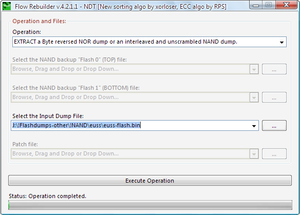
- (NAND only) UNSCRAMBLE then interleave two NAND flashes into one unified dump - (4.1.0.0 and higher) : Makes a unified dump.bin from 2 seperate NAND flash dumps.
- In the second step it also extract the content of the unified dump. Make sure it extracts correctly (it will give no warning if it fails!) and all the needed files are there.
- (NAND only) RE-SCRAMBLE a modified dump then de-interleave it into two new flashes - (4.1.0.0 and higher) : Splits the unified dump.bin into 2 new seperate NAND flash dumps.
- Byte reverse and EXTRACT a NOR dump file - (4.1.0.0 and higher) : First byte reverse the single dump.bin then extract NOR content.
- EXTRACT a Byte reversed NOR dump or an interleaved and unscrambled NAND dump - (4.1.0.0 and higher) : Extract the single dump.bin.
- Byte reverse and PATCH a NOR dump - (4.2.1.1 and higher).
- PATCH a Byte reversed NOR dump or an interleaved and unscrambled NAND dump - (4.2.1.1 and higher).
- Byte reverse a dump - (4.2.1.1 and higher).
Note: when getting errors with autopatcher, use Winskeet to patch the unified dump and then Flowrebuilder to Rescramble it. -> Fixed in FlowRebuilder v.4.2.1.2
Extracted flash content files
(make sure they are all there, flowrebuilder will not give warning when it fails!):
- bootloader_0
- bootloader_1 (NAND only)
- cCSD
- cISD
- creserved_0 (NAND only)
- cvtrm
- eEID
- trvk_pkg
- trvk_prg
- \asecure_loader\metldr
- \ros\[two seperate folders named to FW version]\CoreOS files (19 up to 25 files, depending the FW version)
Notes:
- if it only extracted bootloader_0 + bootloader_1, check that both NANDs are dumped correct (known error with flashers that has bug with second NAND channel to read), and that high/low where selected correct.
- Do not use spaces in the folderpath, or Flowrebuilder will not extract the files.
- Bug workaround: delete previous extraction attempts to prevent Flowrebuilder to always error. -> bugreport -> Fixed in FlowRebuilder v.4.2.2.0
From unified to seperate low/high NAND files
If for some reason you lose the original seperate low/high NAND files and only have the unified, you need donor files to regenerate them.
extract and in Flowrebuilder select the option "RE-SCRAMBLE a modified dump then de-interleave it into two new flashes"
- Select the NAND backup "Flash 0" (TOP) file : here drop the 1bkp.bin
- Select the NAND backup "Flash 1" (BOTTOM) file : here drop the 2bkp.bin
- Select the Input NAND interleaved Modified file : here drop your unified flash .bin file
and click Execute Operation
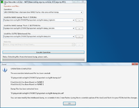
This will result in making 2 new deinterleaved files you could use for reflashing (it is recommended to alway use your own deinterleaved sourcedumps, this method is only mentioned as last resort for people that lost their backups).
Online help
Upload your dump to a fileshare host (e.g. http://www.mediafire.com/ or http://www.mirrorcreator.com/) and join IRC ef.net in channel #ps3downgrade (tip: use a real IRC client e.g. Xchat-WDK instead of webhosts like mibbit)
Note: when uploading NAND dumps, make sure to upload the seperate NAND files, not the unified! This makes it easier to trace user errors in the descrambling/unification process.
Please use this method only after you first tried the above options first (so you have learned from it as well) :) Tip: look on talkpage for a step by step guide (and please improve where possible).


