USB: Difference between revisions
Jump to navigation
Jump to search
m (CECHCxx and CECHExx uses the same motherboard) |
m (Text replacement - "!important!important" to "!important") |
||
| (6 intermediate revisions by 2 users not shown) | |||
| Line 1: | Line 1: | ||
= USB 2.0 = | = USB 2.0 = | ||
<div style="float:right">[[File:CECHC GL852- IC3305.JPG|200px|thumb|left|[[GL852]] USB-Hub 64-pin as seen on [[CECHCxx]]]]</div> | |||
Depending on the [[SKU Models]] the PS3 is equiped with 6x (Tool/DECR), 4 or 2 [http://en.wikipedia.org/wiki/USB USB (Universal Serial Bus)] 2.0 ports with maximum bandwidth of 480 Mbit/s (~57 MB/s), connected internally to a USB-Hub chip. | Depending on the [[SKU Models]] the PS3 is equiped with 6x (Tool/DECR), 4 or 2 [http://en.wikipedia.org/wiki/USB USB (Universal Serial Bus)] 2.0 ports with maximum bandwidth of 480 Mbit/s (~57 MB/s), connected internally to a USB-Hub chip. | ||
'''Note:''' On PS3 Slim [[CECH-20xx]]/[[DYN-00x|DYN-001]] and later, the USB port datalines are directly connected to [[South Bridge]] without a USB-Hub chip (port is initialised via DC switch IC connected to [[South Bridge]] and TH3301 thermistor protect 5V input). | '''Note:''' On PS3 Slim [[CECH-20xx]]/[[DYN-00x|DYN-001]] and later, the USB port datalines are directly connected to [[South Bridge]] without a USB-Hub chip (port is initialised via DC switch IC connected to [[South Bridge]] and TH3301 thermistor protect 5V input). | ||
For more detailed info about the USB hub pinout see: [[GL852]] | |||
<gallery> | <gallery> | ||
File:DYN-001 USB lines (top view).jpg|USB lines top view (common traces for all slim models) | File:DYN-001 USB lines (top view).jpg|USB lines top view (common traces for all slim models) | ||
| Line 24: | Line 25: | ||
| 1 || style="color:white; background-color:#CC3333;" | Red || V<sub>BUS</sub> || Power / +5 volt DC (max.500mA) | | 1 || style="color:white; background-color:#CC3333;" | Red || V<sub>BUS</sub> || Power / +5 volt DC (max.500mA) | ||
|- | |- | ||
| 2 || style="color:black; background-color:white;" | White || D- || rowspan="2" | USB 2.0 differential pair | | 2 || style="color:black!important; background-color:white;" | White || D- || rowspan="2" | USB 2.0 differential pair | ||
|- | |- | ||
| 3 || style="color:white; background-color:#33CC33;" | Green || D+ | | 3 || style="color:white; background-color:#33CC33;" | Green || D+ | ||
| Line 41: | Line 42: | ||
| 1 || style="color:white; background-color:#CC3333;" | Red || V<sub>BUS</sub> || Power | | 1 || style="color:white; background-color:#CC3333;" | Red || V<sub>BUS</sub> || Power | ||
|- | |- | ||
| 2 || style="color:black; background-color:white;" | White || D- || rowspan="2" | USB 2.0 differential pair | | 2 || style="color:black!important; background-color:white;" | White || D- || rowspan="2" | USB 2.0 differential pair | ||
|- | |- | ||
| 3 || style="color:white; background-color:#33CC33;" | Green || D+ | | 3 || style="color:white; background-color:#33CC33;" | Green || D+ | ||
| Line 50: | Line 51: | ||
|- | |- | ||
|}'''Note:''' used on many [[Peripherals]] for charging/sync | |}'''Note:''' used on many [[Peripherals]] for charging/sync | ||
{{Motherboard Components}}<noinclude>[[Category:Main]]</noinclude> | {{Motherboard Components}}<noinclude>[[Category:Main]]</noinclude> | ||
Latest revision as of 06:16, 1 July 2023
USB 2.0[edit | edit source]

Depending on the SKU Models the PS3 is equiped with 6x (Tool/DECR), 4 or 2 USB (Universal Serial Bus) 2.0 ports with maximum bandwidth of 480 Mbit/s (~57 MB/s), connected internally to a USB-Hub chip.
Note: On PS3 Slim CECH-20xx/DYN-001 and later, the USB port datalines are directly connected to South Bridge without a USB-Hub chip (port is initialised via DC switch IC connected to South Bridge and TH3301 thermistor protect 5V input).
For more detailed info about the USB hub pinout see: GL852
USB lines top view (common traces for all slim models)
USB lines bottom view (common traces for all slim models)
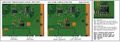
JSD-001/JTP-001 USB connector TH3301 thermistor and DC switch IC to South Bridge
.jpg)
.jpg)
Generic USB Pinout[edit | edit source]

| Pin | Color | Signal | Description |
|---|---|---|---|
| Shell | N / A | Shield | Metal housing |
| 1 | Red | VBUS | Power / +5 volt DC (max.500mA) |
| 2 | White | D- | USB 2.0 differential pair |
| 3 | Green | D+ | |
| 4 | Black | GND | Ground |
| Pin | Color | Signal | Description |
|---|---|---|---|
| Shell | N / A | Shield | Metal housing |
| 1 | Red | VBUS | Power |
| 2 | White | D- | USB 2.0 differential pair |
| 3 | Green | D+ | |
| 4 | N / A | ID | Permits detection of which end of a cable is plugged in: • "A" connector (host): connected to the signal ground • "B" connector (device): not connected |
| 5 | Black | GND | Ground |
Note: used on many Peripherals for charging/sync
| |||||||||||||||||||||||||||||||||||||||||||||||||||||||||||||||||||||||||||||||||||||||||||||||||||||||||||||||||||||||||||||||||||||||||||||||||||||||||||||||||||||||||||||
